
© 2019 IOP Publishing Ltd
1. Introduction
Since the discovery of fullerenes [1], the family of
nanocarbon allotropes has been studied extensively
due to the carbon–carbon bond versatility [2, 3],
with carbon nanotube (CNT) and graphene being
the most well-known [4, 5]. The superior properties
of these nanocarbon materials such as their large
surface-to-volume ratios, electrical and thermal
transport, tunability of band structure by applied
voltage [6–8], magnetic field [9, 10], and mechanical
strain [11–13], as well as synthesis methods have paved
the way for practical applications in nanoelectronics,
electrochemistry, sensors, and supercapacitors
[14–17]. However, such properties have not been
fully exploited in many potential applications. This is
partly due to the non-uniformity of the synthesized
nanocarbon [18, 19], resulting from the non-
ideal interface between the nanocarbon and other
constituent materials [20–26]. For example, CNT
has long been considered as a promising material to
replace copper in on-chip interconnects as the current
density in copper lines exceeds its current-carrying
capacity [27–30]. In reality, although researchers
have demonstrated CNT vias down to sub-100 nm
dimensions [31–33], the resistance of the CNT vias
is still much larger than that of mainstream copper
interconnects. Such large interconnect resistance is
mainly due to contact resistance between the CNTs
and other conductors [21, 22, 24, 34]. Many efforts
have been devoted to reducing the contact resistance
for carbon-based electron devices [35]. Since both
W Du et al
042005
2D MATER.
© 2019 IOP Publishing Ltd
6
2D Mater.
2DM
2053-1583
10.1088/2053-1583/ab41d3
4
1
16
2D Materials
IOP
23
September
2019
Structures, properties, and applications of CNT-graphene
heterostructures
Wei Du
1
, Zubair Ahmed
2
, Qi Wang
1
, Cui Yu
3
, Zhihong Feng
3
,
6
, Guoyuan Li
1
, Min Zhang
4
,
Changjian Zhou
1
,
6
, Richard Senegor
5
and Cary Y Yang
5
1
School of Microelectronics, South China University of Technology, Guangzhou 510641, People’s Republic of China
2
Department of Electronic and Computer Engineering, The Hong Kong University of Science and Technology, Kowloon, Hong Kong,
People’s Republic of China
3
National Key Laboratory of ASIC, Hebei Semiconductor Research Institute, Shijiazhuang 050051, People’s Republic of China
4
School of Electronic and Computer Engineering, Peking University, Shenzhen 518055, People’s Republic of China
5
Center for Nanostructures, Santa Clara University, Santa Clara, CA, United States of America
6
Authors to whom any correspondence should be addressed.
E-mail: [email protected] and [email protected]
Keywords: graphene, carbon nanotube, heterostructure, interconnect, electron transport, thermal transport
Abstract
Both carbon nanotube (CNT) and graphene exhibit excellent properties and have many potential
applications in integrated circuits, composite materials, thermal management, sensors, energy
storage, and flexible electronics. However, their superior properties are confined to one or two
dimensions, thus limiting their utility in interconnects or thermal interface materials that require a
3D structure for efficient electron and/or phonon transport. It is conceivable that a combined CNT-
graphene structure would provide new opportunities for realizable applications in these and other
fields. In recent years, numerous results on synthesis, structural analyses, theoretical modeling, and
potential applications of various CNT-graphene heterostructures have been reported. In this review,
we summarize the possible structures that can be formed by connecting CNT and graphene. We then
report existing experimental efforts to synthesize the heterostructures based on growth method,
catalyst design, and the resulting properties. Also, theoretical studies on various heterostructures
are reviewed, with the focus on electron and thermal transport within the heterostructure and
across the CNT-graphene interface. Several potential applications are briefly discussed, and a
combined theoretical and experimental approach is proposed with the objective of enhancing the
understanding of the CNT-graphene heterostructure and attaining a realistic assessment of its
feasibility in practical applications.
TOPICAL REVIEW
2019
RECEIVED
20 May 2019
REVISED
20 August 2019
ACCEPTED FOR PUBLICATION
5 September 2019
PUBLISHED
23 September 2019
https://doi.org/10.1088/2053-1583/ab41d3
2D Mater. 6 (2019) 042005

2
W Du et al
graphene and CNT have the same honeycomb
structure, a seamless contact between them appears
possible [36]. A 3D all-carbon structure consisting of
CNT-on-graphene could realize excellent electrical
and thermal conduction in both horizontal and
vertical directions. Such a structure could then serve as
a building block in on-chip interconnects.
In applications that aim to take advantage of
the large surface-to-volume ratio in CNT and gra-
phene, such as electrodes in supercapacitors, batter-
ies, and reactive catalysts [37–39], it is challenging to
prevent the aggregation of the nanocarbons [40, 41].
In contrast, if a heterostructure consisting of verti-
cal CNT arrays and horizontal graphene layers is
formed, a more robust structure is expected to resist
the aggregation tendency while still preserving the
high surface-to-volume ratio [42, 43], electrical and
thermal transport [44, 45], optical and optoelectronic
properties [46], and tunability of band structure by
applied volt age [6–8] and magnetic field [9, 10, 47].
With the objective to fully exploit the extraordi-
nary properties of nanocarbons, researchers in various
disciplines, including electronics [48, 49], material sci-
ence [50], mechanical engineering [51], and chemistry
[52], have explored the possibility of combining these
two most well-known nanocarbon allotropes during
the last decade. Therefore, it is meaningful to review
what has been achieved, and what can be expected in
future studies of the CNT-graphene heterostructure.
This paper is organized as follows. The next sec-
tion describes the basic structures of and synthesis
methods for CNT-graphene heterostructures, fol-
lowed by a review of theoretical studies based on
techniques including first-principle calculations and
molecular dynamics simulations. We then present
various potential applications of the heterostruc-
tures. Finally, we conclude with a discussion of what is
needed to fully optimize the heterostructure for practi-
cal applications.
2. Structures and growth methods
2.1. Structures
To make full use of the structure and properties of the
1D CNT and 2D graphene, various methods have been
proposed to prepare CNT arrays [53], while graphene,
with its 2D planar structure, is usually grown on metal
foils or thin films [54]. Although both show promise
in many applications, it is beneficial to combine them
into a single CNT-graphene heterostructure, which
not only preserves the excellent properties of the
two materials, but also compensates for each other’s
shortcomings to some extent. Generally, CNT grows
along the axial direction, thus forming CNT arrays
vertical or parallel to the substrate. Several possible
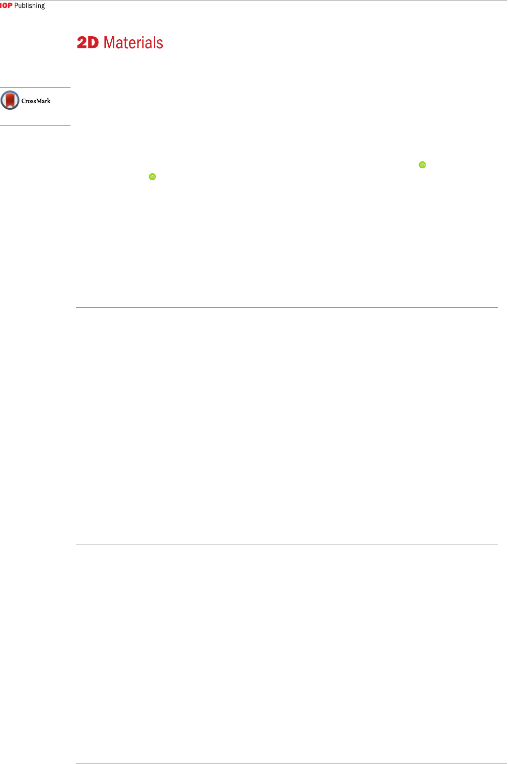
models of joining CNTs and graphene are illustrated
in figure 1. A parallel CNT-graphene heterostructure
[55–58] (figure 1(a)) can be obtained by drop-casting
CNT on the transferred graphene, or graphene can
be transferred to cover the CNT network to form a
similar structure but with graphene on top [59]. While
these two structures preserve the 2D structure as in
graphene, it is desirable to form a truly 3D structure by
joining vertical CNTs and planar graphene. Figure 1(b)
shows a typical structure with the CNT axis normal
to the graphene plane [42, 60–65], forming a vertical
CNT-graphene heterostructure. In certain cases, the
graphene can be lifted off during the CNT growth, thus
forming a structure as shown in figure 1(c) [66–69].
Recently, several experimental works claimed to obtain
seamless CNT-graphene heterostructures [36, 70]
(figures 1(d) and (e)). Multilayered vertical CNT-
graphene heterostructure was also reported as an all-
carbon pillared structure [71] (figure 1(f)), in which
graphene was used as the platform for CNT growth
and the grown CNTs served as pillars to support
graphene layers. In principle, the seamless junctions
between CNT and graphene can yield a more robust
mechanical structure with enhanced interplanar
electrical and thermal conduction.
In general, compared to the parallel CNT-graphene
heterostructure, the vertical CNT-graphene configu-
ration is more desirable for applications that require
low electrical resistance. Gao [72] compared the resist-
ance of the parallel and vertical CNT-graphene het-
erostructures, and found that the parallel heterostruc-
ture exhibited a contact resistance of 51.9 kΩ, which is
nearly four times the contact resistance of 14 kΩ in the
vertical heterostructure. The difference is likely due to
the unsatur ated π-bonds of edge atoms in the vertical
CNT configuration, giving rise to stronger bonding
with atoms in the graphene layer. Based on the devel-
opment of the different pillared heterostructures,
theoretical and experimental analyses of the CNT-gra-
phene-CNT heterostructure (figure 1(f)) have been
carried out in recent years [52, 71, 72–76].
2.2. Growth methods
As there are many excellent reviews on the growth
of CNT and graphene [53, 77–79], the focus of this
paper is on the growth of the heterostructure itself.
Specifically, we discuss the various parameters for
growth of CNT-graphene heterostructures, including
the overall methodology, catalyst requirement, growth
temperature, and properties of the resulting structure.
2.2.1. Parallel CNT-graphene heterostructures
Parallel CNT-graphene heterostructures are generally
formed using chemical vapor deposition (CVD)
[56, 57, 80]. In such a method, a graphene film is
synthesized first, followed by catalyst deposition on the
graphene and then CNT growth to form the parallel
CNT-graphene heterostructure. For example, using
FeCl
3
solution deposited on graphene as catalyst, CNTs
were formed on the dried sample after the introduction
of argon/hydrogen/acetylene (30/30/5 sccm) at 750 °C
[80]. It was determined that the density and the
quality of the CNTs was related to the concentration
2D Mater. 6 (2019) 042005
3
W Du et al
of the FeCl
3
solution. The density of CNTs can be well
controlled simply by choosing the corresponding
concentration for a targeted density requirement. On
the other hand, the use of the FeCl
3
is avoided in many
cases because of the potentially hazardous waste it
creates. With CNTs as the template, a CNT spider web
was firstly deposited on a copper substrate [56], then a
xylene solution consisting of ferrocene and sulfur was
injected into CNT webs, followed by high-temperature
annealing. The parallel CNT-graphene heterostructure
was then formed with the introduction of a carbon
source, and the CNTs served as nucleation centers
during the graphene growth, as shown in figure 2(a).
This cage-growth method ensures good matching
between CNT network-embroidered graphene film
and graphene, which contributes to the development of
all-carbon devices.
An alternative method used graphene as the
growth template, on which the CNTs were directly
deposited without carbon source gas [57]. It was
found that CNTs in the parallel heterostructure lay
mainly along the armchair axes of the graphene film
(figure 2(b)). To obtain better aligned CNT-graphene
heterostructure, coating the CNTs on graphene was
used, while ensuring that the CNTs and graphene were
firmly connected. Figure 2(c) shows the graphene film
coated with cross-folded CNT networks [81]. After
etching the Cu substrate, a self-standing parallel CNT-
graphene heterostructure was obtained. The CNT-
graphene film obtained by the facile method has ~90%
electron transparency, which is suitable for high-per-
formance electrode applications.
Various methods have been proposed to increase
the CNT density and thus the electrical performance
Figure 1. Schematic illustrations of the (a) parallel CNT-graphene heterostructure, (b) and (c) normal CNT-graphene
heterostructure, (d) and (e) seamless CNT-graphene heterostructure, and (f) CNT-graphene-CNT heterostructure.
Figure 2. Scheme for CNT-graphene parallel heterostructure. (a) Graphene grown by Chemical Vapor deposition using CNTs
as templates [56]. (b) CNTs grown by Chemical Vapor deposition using graphene film as template [57]. (c) Cross-staking CNT
networks coated on the graphene film [81]. (d) By blown bubble method [55].
2D Mater. 6 (2019) 042005
4
W Du et al
of the resultant heterostructure. Wu [55] adopted a
blown bubble method to prepare the aligned CNT
arrays on top of graphene (figure 2(d)). Multiwall
CNTs (MWCNTs) were grown first, and a CNT solu-
tion with PMMA and acetone as the solvent was pre-
pared to form the bubble solution. Aligned CNTs were
obtained due to surface tension of the bubble. The
CNT density was increased by simply repeating the
bubble transferring process. The final high-temper-
ature annealing process could enhance the bonding
between CNT and graphene, which is beneficial for
electrical and thermal applications.
2.2.2. Vertical CNT-graphene heterostructure
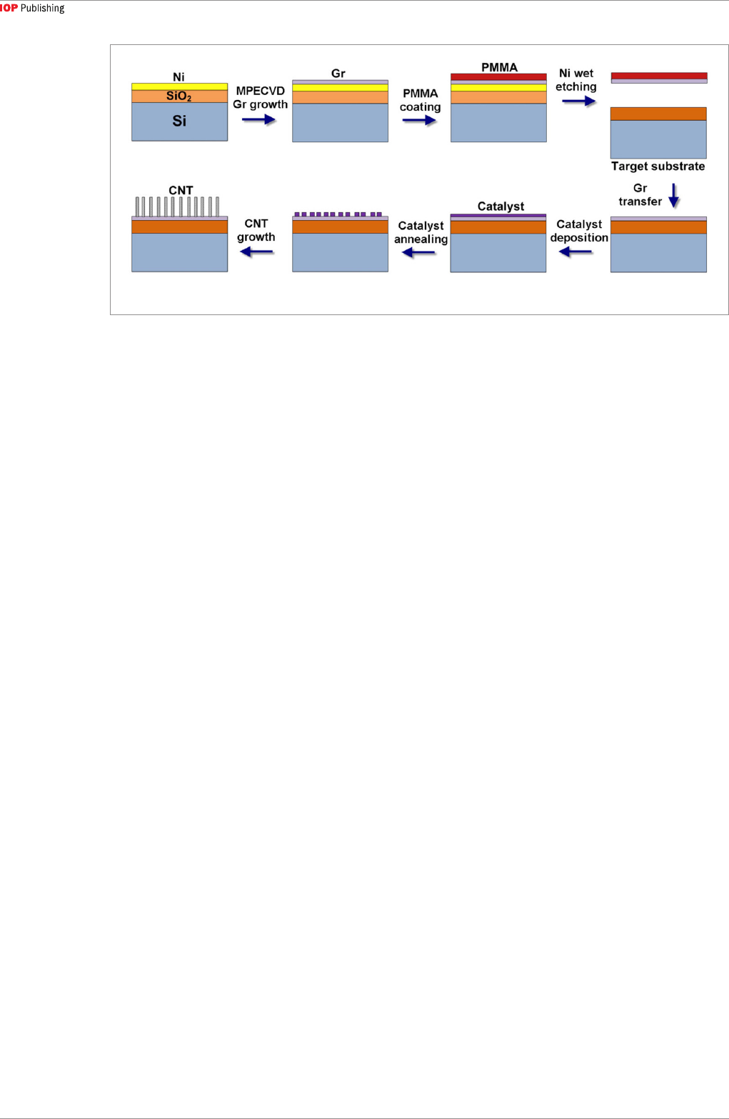
In general, CVD [50, 81–88] is the most common
method for synthesizing vertical CNT-graphene
heterostructures, using a two-step process as
illustrated in figure 3 [89]. First, graphene is grown on
a metal substrate and subsequently transferred onto a
target substrate if needed. Second, the vertical CNT-
graphene heterostructure is synthesized after catalyst
deposition and introduction of a carbon source gas.
There are many factors that affect the growth, and
we will focus on the effects of catalysts, temperature,
and gases on the characteristics of the resulting
heterostructure.
Experiments on the choice of catalyst using differ-
ent thicknesses of Fe or Ni have been carried out [89].
It was found that if the Fe film thickness could be con-
trolled within a range of 0.2 nm to 1 nm, better quality
of CNTs was obtained for thinner films, as confirmed
by Raman analyses. When the Fe film thickness was as
low as 0.5 nm, single-walled CNTs (SWCNTs) were
obtained. Otherwise, MWCNTs resulted whether Fe or
Ni was used as the catalyst [89]. The diameter of the
CNTs is largely affected by the catalyst film thickness.
In addition, the effects of Ni and Fe catalyst on forma-
tion of the CNT-heterostructure are quite different, as
Ni etches graphene during the growth process, leading
to more defects in the final structure. It is worth noting
that the etching of the graphene is expected, because in
the early stages of CNT growth, graphene is a carbon
source in addition to the carbon source gas. And H
2
also plays an important role in the etching of graphene
because of the reaction [63]
(Ni)
nanoparticle
+ C
graphene
+ 2H
2
→ Ni + CH
4
.
The growth temperature and gas feedstock can be
tuned to minimize graphene etching. By using
C
2
H
4
as the carbon source, the Ni catalyst film can form
higher density nanoparticles at 700 °C and the etching
becomes less reactive compared to 800 °C, resulting in
higher density CNTs and less etching of graphene [63].
Apart from graphene etching, catalytic nanopar-
ticles become embedded in the CNT-graphene junc-
tions in some cases, which limits the properties of
the heterostructure. To prevent this effect and form a
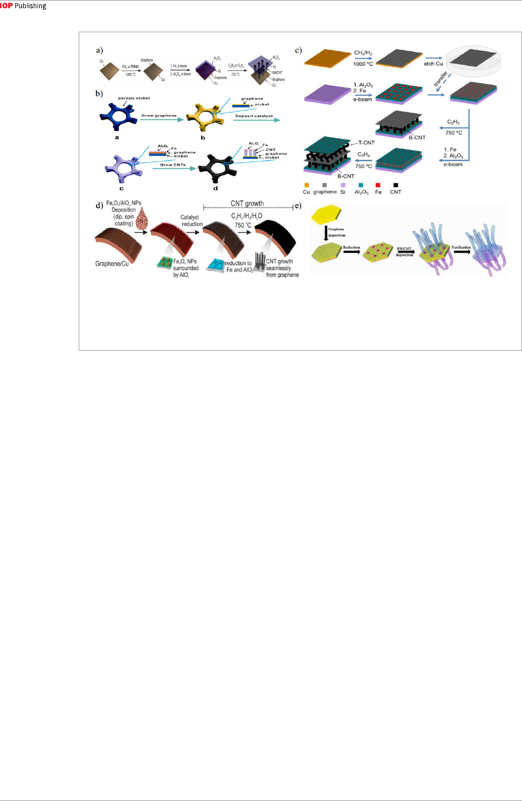
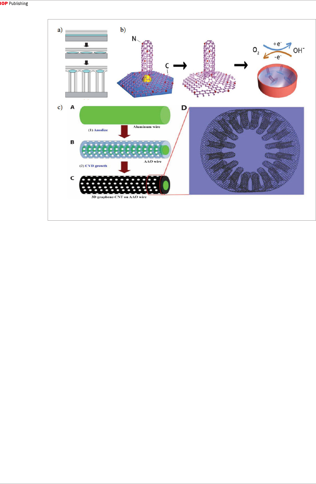
seamless CNT-graphene heterostructure, Zhu [36]
deposited a layer of Al
2
O
3
film on the Fe catalyst film
as a floating buffer layer (figure 4(a)). The floating
buffer was designed to transform the bottom growth
of the CNTs into tip growth, thus achieving the goal
of a seamless CNT-graphene heterostructure with
optimal interface properties. Similarly, the hetero-
structure was successfully [87] synthesized on a porous
Ni foam by using the same method but with a better
area utilization ratio of the metal substrate, as shown in
figure 4(b). Inspired by this method, Jiang [77] realized
that CNTs could grow from both sides of graphene,
as shown in figure 4(c). This unique structure has the
potential to be used in energy storage that requires a
high surface-to-volume ratio.
Instead of using solid catalyst films, Rodrigo [70]
spun a solution of Fe
3
O
4
/AlO
x
nanoparticles as the cat-
alyst on the graphene/Cu substrate, which is also appli-
cable to curved substrates. Being exposed to hydrogen
at 750 °C, the catalyst nanoparticles became a mixture
of Fe and Al
2
O
3
. Then a seamless CNT-graphene het-
erostructure was formed via tip growth mechanism,
with the covalent C–C bonds at the CNT-graphene
junction, as shown in figure 4(d). By using Fe catalyst,
SWCNTs can be grown at 950 °C on a FeMgAl layered
double oxide substrate [90], with the process shown
in figure 4(e). Compared to MWCNT, SWCNT arrays
have a higher surface-to-volume ratio and smaller
Figure 3. A two-step process for CNT-graphene heterostructure preparation [89].
2D Mater. 6 (2019) 042005
5
W Du et al
defect density, while forming covalent C–C bond at
the CNT-graphene interface, leading to better elec-
tron transport [90]. The superior properties of the
SWCNT-graphene heterostructure are suitable for
applications as electrodes in high energy density bat-
teries.
In general, all catalyst film thicknesses in the two-
step method are between 1 and 10 nm or thinner to
yield good-quality CNTs. With increase in catalyst film
thickness, graphene can also be formed. Therefore,
CNT and graphene can be grown simultaneously if the
thickness of the catalyst can be controlled within a few
nanometers. Instead of the two-step growth method,
a one-step method is also feasible for forming verti-
cal CNT-graphene heterostructures, thus simplify-
ing the growth process. Kondo [67] deposited differ-
ent thickness of Co film on 5 nm TiN to form a mixed
catalyst. The thickness of the Co catalyst is within a
few nanometers so that both graphene and CNTs can
be synthesized using Co catalyst. With the gas ratio
of acetylene to argon being 1:9, graphene films were
formed first, then the Co catalyst film dewetted to
form nanoparticles, followed by CNT growth at 510
°C using tip-growth mode and resulting in a vertical
CNT-graphene heterostructure on a silica substrate
(figure 5(a)). It was found that increased Co thickness
resulted in increased graphene thickness.
Ni/TiN was also reported as a catalyst to synthesize
CNTs and graphene [68]. Without conventional argon
pretreatment, Jousseaume [68] used C
3
H
6
as the car-
bon source gas rather than traditional C
2
H
2
or CH
4
,
and prepared a vertical CNT-graphene heterostruc-
ture at 400 °C using bottom-growth mode. The lower
temperature ensures compatibility with chip manu-
facturing processes for the vertical CNT-graphene
heterostructure to serve as part of an on-chip inter-
connect network. Furthermore, using FeMoMgAl lay-
ered double hydroxides as catalyst, a nitrogen-doped
CNT-graphene heterostructure has also been achieved
by the one-step method [91]. The schematic of the
growth process is shown in figure 5(b). The specific
surface area of the structure reached 812.9 m
2
g
−1
and
the electrical conductivity was as high as 53.8 S cm
−1
.
In addition, the structure had excellent bifunctional
oxygen electrode activity for both oxygen reduction
reaction and oxygen evolution reaction, which offers
possibility to be a bifunctional electrocatalyst in metal-
free devices.
Seamless heterostructures can also be obtained by
the one-step method [92]. A typical example is shown
in figure 5(c). First, an aluminum wire was exposed
to 0.3M oxalic acid solution at 40 V and 3 °C so that
the external surface could be turned into anodized
aluminum oxide. Then without catalyst, CNTs were
seamlessly surrounded by a cylindrical graphene layer
using CVD. In general, the key in the one-step growth
is the proper choice of catalyst (material and thickness)
and temperature to form the two constituent nanocar-
bon materials sequentially or simultaneously.
It is expected that the seamless heterostructure
shown in figures 2(d)–(e) can provide superior elec-
tronic and thermal transport properties through the
CNT-graphene junction as well as improved mechani-
cal stability. However, there is still little evidence that
the fabricated vertical structure possesses a seamless
connection. Several proposed connection topologies
Figure 4. Scheme for CNT-graphene vertical heterostructure. (a) Synthesis of CNT carpets directly from graphene by adding a
layer of Al
2
O
3
film on Cu substrate [36]. (b) Synthesis of seamless CNT-graphene heterostructure by adding a layer of Al
2
O
3
film on
porous Ni substrate [87]. (c) CNTs grown from both sides of graphene using supporting layer: Al
2
O
3
films [76]. (d) Using solution
of Fe
3
O
4
/AlO
x
nanoparticles as catalyst [70]. (e) Growing seamless SWCNT-graphene heterostructure on FeMgAl layered double
oxide substrate [90].
2D Mater. 6 (2019) 042005
6
W Du et al
between CNT and graphene are presented in the next
section along with first-principle calculations. How-
ever, high-resolution transmission electron micros-
copy is needed to show experimentally how the carbon
atoms are connected at the CNT-graphene junction.
We hope that with more advanced characterization
techniques, the atomic arrangement at the junction
can be identified, and provide an experimentally con-
firmed structure for theoretical calculations.
3. Theoretical Studies of CNT-Graphene
Heterostructures
Both CNT and graphene have extraordinary electronic
transport properties, mechanical strength, and
thermal conductivity. Until now, various theoretical
methods have been employed to study the properties
of CNT-graphene heterostructure, specifically to
simulate seamless CNT-graphene heterostructures.
In principle, there can be numerous geometrical
configurations for both parallel and vertical CNT-
graphene heterostructures, considering the various
CNT chiralities, the number of walls in a CNT, the
bonding type between CNT and graphene that could
be van der Waals or covalent. Thus, it would not be
practical to list all the possibilities of CNT-graphene
heterostructures. Those that have been studied are
constrained partly by the computational resources and
the difficulty in establishing a stable junction between a
CNT and graphene. Nevertheless, there are interesting
properties revealed by various theoretical studies,
though most remain unverified by experiment.
3.1. Parallel CNT-graphene heterostructure
As the parallel CNT-graphene heterostructure is
mainly used for electrodes or all-carbon transistors,
most theoretical studies have focused on its electronic
properties [93–95]. Ho [93] studied the electronic
structures of a non-chiral (armchair or zigzag type)
CNT positioned flat on the underlying graphene,
as shown in figure 6(a). The exact position of CNT
is optimized using the Lennard-Jones interatomic
potential, and the interlayer distance between CNT
and graphene is around 3.1 Å–3.2 Å, implying that
the bonding is van der Waals type. Compared to
pristine CNT and graphene, the band structure of
the heterostructure exhibits typical coupling effects
between CNT and graphene, resulting in extra band-
edge states at the intersecting linear bands, as shown
in figure 6(b). The coupling effect can be further
modulated by rotating the CNT relative to the in-
registry position, but it generally weakens as the CNT
diameter and the interfacial distance increases. One
interesting phenomenon is the induced non-zero
bandgap for pristine metallic (3m, 0) CNT due to
coupling to the graphene, suggesting that even metallic
CNT can be used for transistors if the CNT diameter
is small and graphene is used as an underlying
substrate. Similarly, Cook [94] calculated the charge
redistribution between graphene and semiconducting
(8,0) and (10,0) CNTs, and reported a very low
Schottky barrier height between CNT and graphene.
This is qualitatively verified by experimental results of
Chai [96, 97], who applied graphitic interfacial contact
layer to improve the CNT transistor properties, and of
Figure 5. (a) Scheme of one-step method process [68]. (b) Process of the nitrogen-doped graphene/carbon nanotube hybrids
growth [91]. (c) Schematic of radially aligned CNTs growth process [92].
2D Mater. 6 (2019) 042005
7
W Du et al
Ganggavarapu [96, 97], who achieved ohmic contact
between CNT and few-layer graphene.
A seamless parallel CNT-graphene heterostruc-
ture with a (12,0) CNT covalently bonded to one or
more graphene nanoribbons with the same width as
the CNT length has been proposed [98–100]. A com-
mon feature of these structures is the sp
3
-like bonding
at the interface between CNT and graphene. Artyukh
[100] studied the structure where the atoms at the
edge of the two graphene nanoribbons are directly
connected to the CNT wall, as shown in figure 6(c).
Compared to pristine CNT or graphene, the den-
sity of states (DOS) of the heterostructure exhibits
some similar Van Hove peaks, and resemble those in
hydrogenated CNT, as shown in figure 6(d). In terms
of mechanical strength, the heterostructure exhibits
much higher Young’s modulus due to the sp
3
bonds
present at the interface [100].
3.2. Vertical CNT-graphene heterostructure
Vertical CNT-graphene heterostructures have
potential applications in many fields such as
electrodes, interconnects, transistors, catalyst, and
thermal interface materials. Thus, the electronic and
thermal transport properties are of much interest for
these applications. In this sub-section, we focus mainly
on the properties of modeled seamless vertical CNT-
graphene heterostructures to examine its electronic
and thermal transport properties.
To form a seamless CNT-graphene heterostructure,
a least-square method is utilized to achieve C–C bond-
lengths or bond-angles as close as possible to those of
the ideal case [101, 102]. Moreover, Euler’s theorem is
utilized to select the polygons for the contact stitching
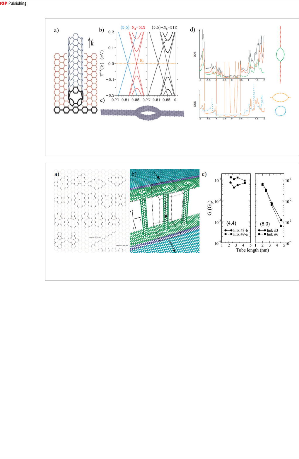
process [101–106]. Figure 7(a) shows the possible con-
nections that the eight open bonds of a (4,4) CNT or (8,
0) CNT can form with the underlying graphene sheet
[101]. Many theoretical calculations have adopted the
same rules to form seamless CNT-graphene hetero-
structures [71, 107]. After identifying the bond contact
spots on the graphene surface and the CNT, molecular
dynamic simulations are performed to minimize the
total binding energy of the heterostructure. For struc-
ture relaxation, a full quantum mechanical optim-
Figure 6. (a) Parallel CNT-graphene heterostructure with Van der Waals bond between CNT and graphene [93]. (b) Band
structures of the CNT, graphene, and coupled CNT-graphene heterostructure [93]. (c) Parallel CNT-graphene heterostructure with
covalent bond between the CNT and graphene nanoribbons at the two sides [100]. (d) Theoretical density of states (DOS) of the
covalent bonded CNT-graphene heterostructure, the DOS of a hydrogenated CNT is plotted in the lower panel as a reference [100].
Figure 7. (a) Possible ways to seamlessly connecting (4,4) or (8,0) CNT with graphene [101]. (b) Graphene-CNT-graphene
heterostructure used to calculate the transmission coefficient, with the arrows showing the electron transport directions [49].
(c) Deduced conductance of the heterostructure with different CNT type and tube length [49].
2D Mater. 6 (2019) 042005

8
W Du et al
ization including force-field relaxation of the nuclei
as well as the electrons is necessary. However, such
optim ization requires prohibitive amount of time and
computational resources [108]. Therefore, another
approach is employed to achieve force-field conv-
ergence using classical molecular dynamics approach,
which neglects electron interactions [89, 109, 110]. The
advantage of such an approach is drastically reduced
computational time, albeit with less accuracy of the
final optimized structure.
3.2.1. Electronic transport properties
With the optimized heterostructure, one can perform
first-principle calculations to obtain electronic
properties such as band structure, transmission
coefficient, DOS, and conductance. Matsumoto [83]
used a tight-binding method to study various (6,6)
CNT-graphene heterostructures, including CNT with
open tip or capped, and CNT sandwiched between two
graphene layers similar to that in figure 1(f). The total
energy minimization method is adopted to optimize
the geometries using the tight-binding method.
Although the (6,6) CNT is metallic, sizable direct
bandgaps of 0.27 eV and 0.51 eV were predicted for
the open and capped CNT-graphene heterostructures,
respectively. An even larger bandgap was predicted for
the sandwiched heterostructure. Another interesting
structure proposed by Mao [111] also showed a similar
effect that the metallic (5,5) CNT was transformed
into a semiconductor with a bandgap of 0.2 eV.
Strictly speaking, this structure is not a seamless
CNT-graphene heterostructure, because the CNT
is inserted into the graphene and the two ends of the
CNT are connected to the graphene sheets through a
hole on each. Nevertheless, a covalent bond is formed
between each atom at the graphene hole edge and
an atom on the CNT sidewall. This strong coupling
results in a bandgap in the metallic (5,5) CNT. In
contrast, the original bandgap of 0.65 eV vanishes for
a semiconducting (8,0) CNT, because of the induced
impurity states by the sp
3
-like hybridization between
the CNT and the holed graphene. Thus, one may
conclude from the above theoretical study that the
pristine CNT bandgap can be changed due to the
strong covalent bond formed at the CNT-graphene
interface.
Since the tight-binding method could not capture
the junction-induced band offset between CNT and
graphene [83], a first-principle calculation was per-
formed by Frederico [49] to study the electronic trans-
port properties of the (4,4) and (8,0) CNT-graphene
heterostructures. For the metallic (4,4) CNT-graphene
heterostructures, two kinds of symmetrical connec-
tions containing six heptagonal rings at the interface
(No. 3 and No. 9 in figure 7(a)) were adopted. The unit
cell of the periodic 3D seamless heterostructure shown
in figure 7(b) was constructed for electronic transport
calculations using the non-equilibrium Green’s func-
tion (NEGF) method, and the current flow is through
the CNT-graphene junction and the CNT itself. The
calculated transmission coefficient was between 0.01
and 1 and shows a weak dependence on the CNT
length in the range of 2.2–4.2 nm, indicating a clear
ballistic transport characteristic of the (4,4) metal-
lic CNT-graphene heterostructure. The conductance
deduced from the transmission curves also shows a
similar weak dependence on CNT length for metallic
CNTs as shown in figure 7(c). On the other hand, the
conductance shows strong dependence on the contact
structure, with the No. 9 contact structure exhibiting
a higher transmission and conductance than the No.
3 case. In contrast, the conductance of the semicon-
ducting (8,0) CNT-graphene heterostructure shows
a strong dependence on the CNT length and weak
dependence on the contact structure. Another interest-
ing point for the (8,0) CNT-graphene heterostructure
is that a relatively large conductance is predicted for
the heterostructure with a small CNT length of 2 nm
(figure 7(c)), showing the effect of tunneling. Although
the study reveals some interesting electronic transport
properties of the CNT-graphene heterostructure, their
calculation cannot ascertain the exact contribution of
the CNT-graphene junction to the total conductance.
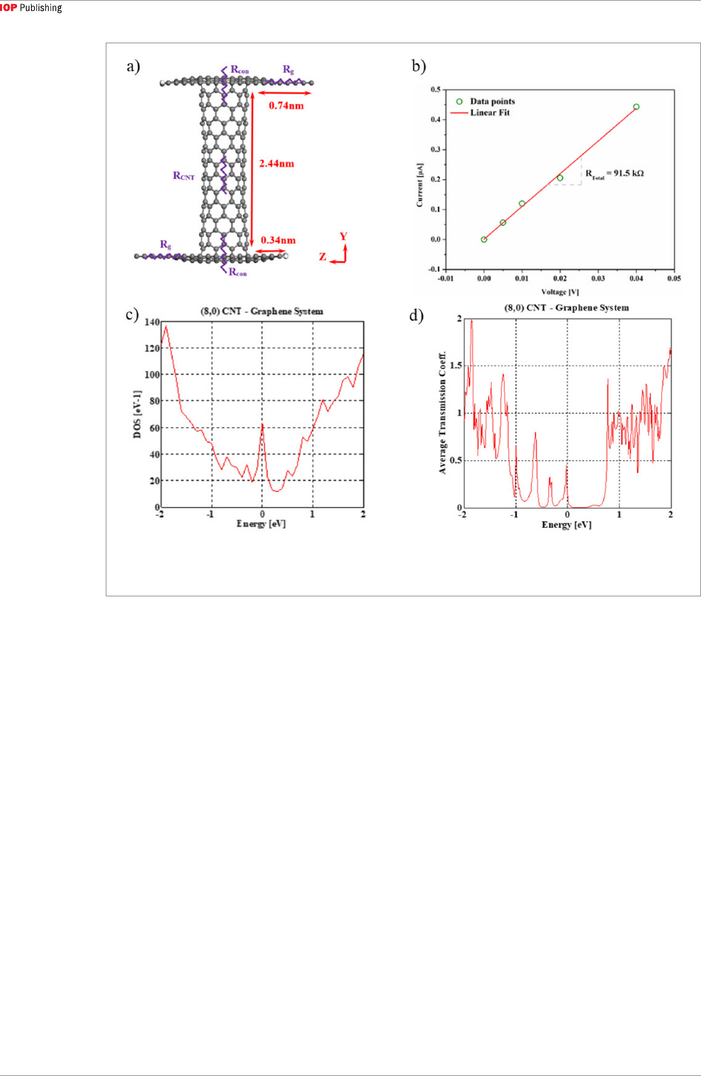
To better understand the CNT-graphene contact
properties, we have performed calculations on a two-
point structure with the NEGF method. To extract the
CNT-graphene contact resistance, graphene resistance,
and CNT resistance, we calculate the current–voltage
(I–V) characteristics of the graphene-CNT-graphene
heterostructure shown in figure 8(a). Toward this end,
we first compute the resistance of a graphene sheet for
different lengths, which turns out to be 6.45 kΩ and
independent of length, confirming ballistic transport.
This result also serves as a validation of the calcul-
ation method. A typical I–V curve for the complete
two-point structure is shown in figure 8(b). The total
resistance is found to be 91.5 kΩ for the heterostructure
with a 2.44 nm long (8,0) CNT. The linear I–V behavior
indicates ohmic conduction across the CNT-graphene
junction and possibly along the CNT as well. Further-
more, we have also verified the previous study that
semiconducting CNTs when contacted with graphene
leads to metallic behavior. The DOS and the transmis-
sion coefficients of the (8,0) CNT-graphene hetero-
structure are shown in figures 8(c) and (d), respectively.
A finite DOS exists at the Fermi-level (located at 0 eV),
representative of the metallic nature of the CNT. The
transmission coefficient shown in figure 8(d) also sug-
gests that transmission indeed occurs at the Fermi-level
because of the available states.
3.2.2. Thermal transport properties
Both CNT and graphene possess outstanding
intrinsic thermal conductivity, but the high thermal
conductivity is only achievable along the CNT length
and in-plane directions in graphene. Vertical CNT
arrays have been considered as a good thermal interface
material (TIM) for its high thermal conductivity along
2D Mater. 6 (2019) 042005
9
W Du et al
its length [112]. However, the interface between the
CNT and the substrate constitutes much of the thermal
resistance, which limits the overall performance
of the thermal interfacial layer. Recently, many
theoretical works have studied the seamless 3D CNT-
graphene heterostructure for its superior thermal
transport properties [74, 75, 113]. The heat flow in
the 3D seamless CNT-graphene heterostructure was
determined to be analogous to current flow [75].
Varshney [75] compared the thermal conduc-
tivity k of the heterostructure with an eight-layer
graphite and a pure (6, 6) CNT. The in-plane thermal
conductivity k
//
of the heterostructure is inferior to
that of an eight-layer graphite, and it increases lin-
early with the distance between adjacent CNTs in the
heterostructure. This can be due to the presence of
less scattering sites for a larger CNT-CNT distance.
The out-of-plane thermal conductivity k
⊥
follows
a similar trend that a larger CNT length results in
a larger k
⊥
. While CNT-CNT distance affects the
overall cross-sectional area of the heterostructure,
the CNT length determines the phonon scattering
length between the two CNT-graphene junctions
separated by one vertical CNT. In general, the k
//
is
much higher than the k
⊥
. For example, the k
//
and k
⊥
are 9.6 W (m K)
−1
and 2.25 W (m K)
−1
, respectively,
for a heterostructure with a CNT-CNT distance of 9
Å. Thus, the two factors must be optim ized to obtain
an overall high k in both directions for practical
applications.
Chen [74] compared k
⊥
of a seamless (6,6) CNT-
graphene heterostructure with the pristine graphene,
and found that the former is at least one order of mag-
nitude larger than the latter. k
⊥
increases with increas-
ing CNT densities, and it reaches about 100 W (m K)
−1
when the density of CNT is about 10%. For efficient
cooling of a hot surface, the heterostructure could
be immersed into a liquid to speed up heat dissipa-
tion [114]. To identify the contribution of the CNT-
graphene junction to the total thermal resistance, Shi
[115] analyzed the temperature profile throughout
the heterostructure, and found that the temperature
jump at the junction contributed to most of the total
thermal resistance. The calculated covalent CNT-gra-
phene junction resistance of 4.1 × 10
−11
m
2
K W
−1
~ 7.2 × 10
−11
m
2
K W
−1
is much lower than those of
other thermal interface materials. On the other hand,
if CNT is weakly connected to the graphene by van der
Waals bond, the calculated junction resistance surged
up to 4 × 10
−8
m
2
K W
−1
, clearly suggesting seamless
covalent bonding between CNT and graphene facili-
tates phonon transport from in-plane direction to out-
Figure 8. (a) Graphene-CNT-graphene heterostructure used for I–V calculations. (b) I–V curve of the graphene-CNT-graphene
heterostructure. (c) DOS and (d) transmission coefficients of the (8,0) CNT graphene system, showing finite DOS and transmission
at Fermi-level (0 eV).
2D Mater. 6 (2019) 042005

10
W Du et al
of-plane direction. A practical application was con-
sidered by Bao [116], who studied the CNT-graphene
heterostructure for heat dissipation from a silicon
substrate. Compared to the CNT-silicon interface, the
insertion of a graphene layer between CNT and silicon
improved the thermal conductance by more than 40%
[116]. Although most of the theoretical study con-
structed similar seamless CNT-graphene structures as
described above, Zhang [113] proposed a novel struc-
ture with a transition cone area between the vertical
CNT and the parallel graphene so that the contact area
could be much larger than the CNT area itself. Com-
pared to the normal CNT-graphene heterostructure,
the proposed structure exhibited an improved thermal
conductance, which even outperformed the pristine
20 Å-diameter CNT if the cone radius reaches 40 Å.
These results suggest alternative ways to construct the
CNT-graphene heterostructure, which can be exper-
imentally realized [113].
As alluded in section 2, MWCNTs are quite com-
mon in grown CNT-graphene heterostructures, yet
few theoretical studies on their transport properties
exist, partly due to the computation resources require-
ment to construct and calculate these complex systems.
In terms of the MWCNT–MWCNT contact where
van der Waals bonds are formed between the carbon
atoms at the outer walls, Varshney [117] stressed the
importance of effective contact area which is affected
by diameter, the number of walls, and the curvature
effect in determining the thermal transfer rate across
the contact area. However, there is no reported study
of the seamless MWCNT-graphene heterostructure to
date. With proper structure construction schemes and
powerful computation resources, the more complex
MWCNT-graphene heterostructure could conceiv-
ably reveal new information for comparison with
experiment.
Even though the synthesized heterostructures
are still quite different from the theoretical model
structures, the introduction of the heterostructure is
motivated largely by applications requiring better elec-
tronic and/or thermal transport properties and larger
surface to volume ratio, which cannot be obtained with
only one form of nanocarbon mat erial. As discussed in
the next section, there are potential applications that
show superior properties of the heterostructure. More
studies are needed to relate the measured properties
of micro or macroscale heterostructures to theor etical
predictions based on a single nanoscale CNT-graphene
junction.
4. Potential applications
Due to the excellent properties of graphene and CNTs,
CNT-graphene heterostructures have been proposed
as electrodes, catalysts, as well as materials for hydrogen
storage and interconnects. In this section, examples are
given stressing the advantages of using CNT-graphene
heterostructures for such applications.
4.1. Electrodes
For electrodes, a large and efficient conducting area
is the key parameter. The large conducting surface of
graphene makes it an attractive candidate. However,
because of the aggregation of graphene, electrodes
composed of graphene alone would not be the optimal
choice. Considering the electrical conductivity of
CNTs, the combination of vertically aligned CNTs on
graphene holds great promise as a superior electrode
The CNT-graphene electrode, also called all-carbon
electrode, has more effective conducting surface
than graphene while retaining its high mechanical
flexibility, resulting in larger electron transfer capacity
[65]. In addition, the resistance of the CNT-graphene
heterostructure is smaller than that of the graphene
[72], which can also enhance electronic transmission.
Thus, CNT-graphene electrode can be a great
candidate for supercapacitors [42, 52, 118]. Using
parallel CNT-graphene heterostructure as electrodes
[118], a supercapacitor yielded a specific capacitance
of 290.4 F·g
−1
. Figure 9(a) shows the comparison of
specific capacitances of CNT, graphene, graphene/
CNT composite supercapacitors at different charging
current densities, which indicates the superior
performance of the composite supercapacitor. Using
vertical CNT-graphene heterostructure, a high-
performance supercapacitor has been fabricated with
a capacitance of 385 F·g
−1
at a scan rate of 10 mV·s
−1
in 6M KOH solution, with high electrochemical
stability [52]. Another supercapacitor was reported
to exhibit a capacitance of 653.7 µF cm
−2
at 10 mV
s
−1
, and the capacitance of the heterostructure is
higher than that of graphene, as shown in figure 9(b)
[42]. Besides supercapacitors, the CNT-graphene
electrode can also be applied to solar cell. Because
of the larger conducting surface, the dye-sensitized
solar cell showed a fill factor of 0.7 by using a CNT-
graphene heterostructure as the electrode, as shown in
figure 9(c) [60]. Thus, the enhanced effective surface
area and low resistance can create immense potential
for CNT-graphene electrode in supercapacitors or
solar cells, which are renewable and pollution-free
energy storage devices.
4.2. Catalysts
In recent years, CNT-graphene heterostructure has
also been studied as potential metal-free catalyst [91,
119, 120]. By using the one-step method, SWCNTs and
graphene can grow simultaneously on a graphene oxide
(GO) substrate. By in situ doping in the growth process,
a new N-doped graphene/SWCNT hybrid (NGSH)
material can be obtained [91]. Figure 10(a) shows
that N-doped vertical CNT-graphene heterostructure
electrode has higher current density than vertical Pt/C
electrode [91]. Because SWCNTs have higher surface-
to-volume ratio, this NGSH structure possessed a large
specific surface area of 812.9 m
2
g
−1
and high electrical
conductivity of 53.8 S cm
−1
. It turned out that the
hybrid structure was a high-performance and low-
2D Mater. 6 (2019) 042005
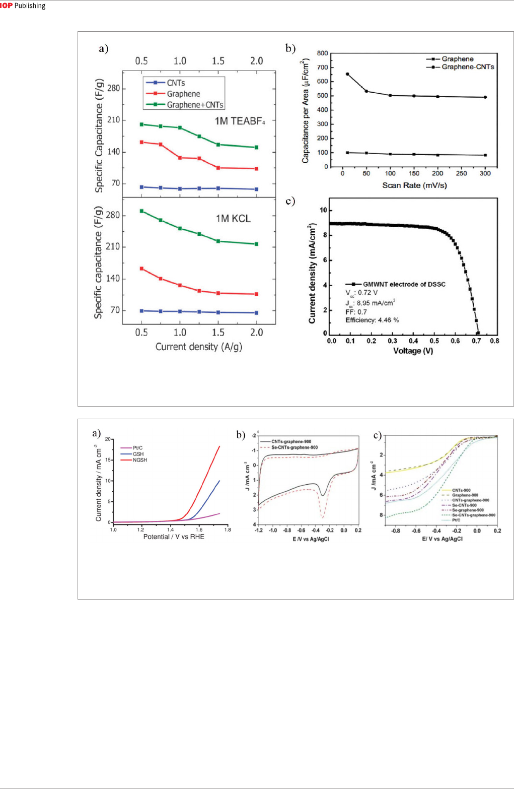
11
W Du et al
cost catalyst for both oxygen reduction reaction and
oxygen evolution reaction. Its high oxygen reduction
reaction activity was even better than the commercial
20 wt% Pt/C catalysts because of its better durability
and low resistance [91]. Apart from N-doped CNT-
graphene heterostructure [91, 119], Se-doped CNT-
graphene heterostructure also showed excellent
electrocatalytic activity [120]. Figures 10(b) and (c)
show that the Se-CNTs-graphene heterostructure has
the lowest resistance. Thus, using novel doping and
growth methods can lead to functionalizing metal-free
catalysts using CNT-graphene heterostructures in the
future.
4.3. Hydrogen storage
It is known that hydrogen can be an energy source, but
its storage capacity is low due to the van der Waals force
between hydrogen molecules and the size of the metal
container. A vertical CNT-graphene heterostructure
can offer an alternative to store hydrogen, as its pore
size and surface area can be adjusted by varying the
growth process parameters. Theoretical study was
conducted and showed that this structure can be
effective in increasing storage capacity [71]. When
doped with lithium cations, this structure yielded
41 g of H
2
/L [71], close to the volumetric requirement
of United States Department of Energy for mobile
Figure 9. (a) Comparison of specific capacitance of CNT, graphene and parallel CNT-graphene heterostructure supercapacitors at
different charging current densities [118]. (b) Capacitance of vertical CNT-graphene heterostructure and graphene at scan rates of
10–300 mV s
−1
[42]. (c) Current density versus voltage behavior of dye-sensitized solar cell with a CNT-graphene electrode [60].
Figure 10. (a) Oxide evolution reduction current density of Pt/C, CNT-graphene and N-doped CNT-graphene electrodes in
0.1 mol l
−1
KOH solution at 5 mV s
−1
[91]. (b) Cyclic voltammetry curves of CNT-graphene heterostructure before and after doping
with Se [120]. (c) Linear sweep voltammetry curves for CNT, graphene and CNT-graphene heterostructure before and after doping
with Se [120].
2D Mater. 6 (2019) 042005
12
W Du et al
applications, which is 45 g of H
2
/L. A simulation of the
stacking of the vertical CNT-graphene heterostructure
for hydrogen storage is depicted in figure 11(a). Thus,
successful fabrication of the stacked CNT-graphene
heterostructure can lead to a new hydrogen storage
device in the future.
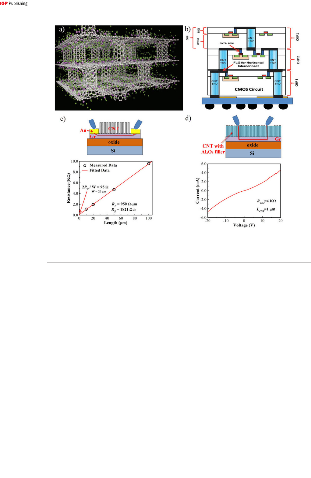
4.4. Interconnects
Continuous downward scaling in chip manufacturing
has become a major challenge for on-chip
interconnects. Due to electromigration challenges,
on-chip Cu interconnect linewidth can no longer
be reduced further in current technology nodes.
Because of their high current capacity and superior
transport properties, graphene [121, 122] and CNTs
[33] have become potential candidates to replace Cu
interconnects. However, the contact resistance between
CNTs and conventional metal is a major challenge
in functionalizing CNT vias [33]. Therefore, an all-
carbon interconnect network consisting of vertical
CNTs on horizontal graphene could mitigate the
contact resistance challenge. Although the contact
between CNTs and graphene can be refined to yield low
resistance and variability, the contact resistivity can only
be low as ~10
−5
Ω cm
2
[66], which is still high. Further,
to facilitate the proper chip operation, CNTs must be
grown on graphene at temperatures compatible to chip
manufacturing, such as 550 °C [48], 510 °C [67] and
400 °C [68]. A schematic diagram for using CNTs and
graphene as interconnects is shown in figure 11(b). The
results in figures 11(c) and (d) suggest that conduction
path does exist in a 3D CNT-graphene heterostructure.
However, contact resistance still remains the critical
challenge in its implementation [89].
5. Summary and conclusions
Structures, growth, properties, and potential
applications of various CNT-graphene hetero-
structures have been reviewed, with emphasis on
targeting a specific performance enhancement for
a given application. For a parallel CNT-graphene
heterostructure, where the CNT axis is parallel
to the graphene plane, the main advantages are
enhanced mechanical strength and increase in
electrical conduction paths, providing a suitable
candidate material for flexible electronics and all-
carbon transistors. For a vertical CNT-graphene
heterostructure, a covalently bonded seamless CNT-
graphene junction has been proposed to reduce the
electrical and/or thermal contact resistance due to its
superior electron and phonon transport properties.
Figure 11. (a) Simulated Li-doped vertical CNT-graphene heterostructure [71]. Green for hydrogen molecules and purple for
lithium atoms. (b) Schematic of vertical CNT-graphene heterostructures as interconnects in CMOS circuit [48]. (c) A schematic of
the electrical measurement and resistance versus graphene length behavior after CNT growth [89]. (d) Schematic of the electrical
measurement and I–V characteristics of the vertical CNT-graphene heterostructure [89].
2D Mater. 6 (2019) 042005

13
W Du et al
Although the structures studied theoretically are
still limited to small-diameter single-walled CNT-
graphene heterojunctions, significant new findings
have been obtained. One example is the opening of a
bandgap for a metallic CNT, while a semiconducting
CNT can be transformed into metallic under certain
heterostructure configurations.
It is well known that controlled synthesis of semi-
conducting CNTs for transistor applications is still
a challenge, while in the case of CNT-graphene het-
erostructures for interconnect applications, semicon-
ducting CNT is not needed. We suggest that future
theoretical study focuses on the transformation of
semiconducting CNT into metallic to support exper-
imental efforts in controlled synthesis. To bridge the
gap between theory and experiment, more theor-
etical studies on MWCNT-graphene heterostructures
should be initiated.
Most of the CNT-graphene heterostructures have
been synthesized by CVD methods, which are usually
adapted from the CNT growth recipes with careful
control of catalyst deposition and catalyst-substrate
interactions. Several works have reported TEM anal-
yses of the CNT-graphene interface in attempting to
reveal the C–C bonding across the interface [48, 60,
67, 70, 86, 123]. Thus far, the experimental findings, in
conjunction with atomistic models used in theoretical
calculations, are still a long way from being conclusive
on the interfacial atomic arrangements. Therefore,
novel techniques are needed to reveal detailed inter-
facial information. For example, the ratio of sp
2
/sp
3
bonding can be extracted from the measured density
of states, if an atomically clean CNT-graphene junc-
tion can be prepared for advanced TEM and STM anal-
yses. The latter poses a great challenge in experimental
study of this heterostructure, while overcoming such
challenge would yield enormous gain in understand-
ing the heterostructure.
Currently, the applications of CNT-graphene het-
erostructures in electronics, thermal interface mat-
erials, and electrochemistry have mainly focused on
macroscale properties, such as electrical and thermal
resistances. In the near future, with more detailed
theoretical investigations and controlled syntheses
of high-quality CNT-graphene heterostructures, we
hope that their superior electron and phonon trans-
port properties can be harnessed to build devices in the
nanoscale, and applications such as nano-transistors,
advanced-node on-chip interconnects, and thermal
interface materials can be realized.
Acknowledgments
This study is supported by National Natural Science
Foundation of China (Grant 11804102), the Science and
Technology Program of Guangzhou (201804010393,
201807010072), Fundamental Research Funds for the
Central Universities and the Key Laboratories Program
(614280104051709). Changjian Zhou would like to
acknowledge the support from Guangdong Pearl River
Youth Talent Recruitment Program.
ORCID iDs
Min Zhang https://orcid.org/0000-0002-2225-
8024
Changjian Zhou https://orcid.org/0000-0002-7156-
348X
References
[1] Kroto H W, Heath J R, O’Brien S C, Curl R F and Smalley R E
1985 C60: buckminsterfullerene Nature 318 162–3
[2] Georgakilas V, Perman J A, Tucek J and Zboril R 2015 Broad
family of carbon nanoallotropes: classification, chemistry, and
applications of fullerenes, carbon dots, nanotubes, graphene,
nanodiamonds, and combined superstructures Chem. Rev.
115 4744–822
[3] Povie G, Segawa Y, Nishihara T, Miyauchi Y and Itami K 2017
Synthesis of a carbon nanobelt Science 356 172–5
[4] De Volder M F L, Tawfick S H, Baughman R H and Hart A J
2013 Carbon nanotubes: present and future commercial
applications Science 339 535–9
[5] Ferrari A C et al 2015 Science and technology roadmap for
graphene, related two-dimensional crystals, and hybrid
systems Nanoscale 7 4598–810
[6] Zhang Y, Tang T-T, Girit C, Hao Z, Martin M C, Zettl A,
Crommie M F, Shen Y R and Wang F 2009 Direct observation
of a widely tunable bandgap in bilayer graphene Nature
459 820–3
[7] Yu Y-J, Zhao Y, Ryu S, Brus L E, Kim K S and Kim P 2009
Tuning the graphene work function by electric field effect
Nano Lett. 9 3430–4
[8] Chen C-W, Lee M-H and Clark S J 2004 Band gap modification
of single-walled carbon nanotube and boron nitride nanotube
under a transverse electric field Nanotechnology 15 1837–43
[9] Chiu Y H, Lai Y H, Ho J H, Chuu D S and Lin M F 2008
Electronic structure of a two-dimensional graphene
monolayer in a spatially modulated magnetic field: peierls
tight-binding model Phys. Rev. B 77 045407
[10] Jarillo-Herrero P, Kong J, van der Zant H S J, Dekker C,
Kouwenhoven L P and De Franceschi S 2005 Electronic
transport spectroscopy of carbon nanotubes in a magnetic
field Phys. Rev. Lett. 94 156802
[11] Chen S, Sun Z and Liu F 2016 Strain engineering of graphene: a
review Nanoscale 8 3207–17
[12] Naumis G G, Barraza-Lopez S, Oliva-Leyva M and Terrones H
2017 Electronic and optical properties of strained graphene
and other strained 2D materials: a review Rep. Prog. Phys.
80 096501
[13] Ni G-X, Yang H-Z, Ji W, Baeck S-J, Toh C-T, Ahn J-H,
Pereira V M and Özyilmaz B 2014 Tuning optical conductivity
of large-scale CVD graphene by strain engineering Adv. Mater.
26 1081–6
[14] Wang C, Takei K, Takahashi T and Javey A 2013 Carbon
nanotube electronics—moving forward Chem. Soc. Rev.
42 2592–609
[15] Avouris P 2010 Graphene: electronic and photonic properties
and devices Nano Lett. 10 4285–94
[16] Lu C-H, Yang H-H, Zhu C-L, Chen X and Chen G-N 2009 A
graphene platform for sensing biomolecules Angew. Chem.,
Int. Ed. 48 4785–7
[17] Tang X, Bansaruntip S, Nakayama N, Yenilmez E, Chang Y-L
and Wang Q 2006 Carbon nanotube DNA sensor and sensing
mechanism Nano Lett. 6 1632–6
[18] Navas H, Picher M, Andrieux-Ledier A, Fossard F, Michel T,
Kozawa A, Maruyama T, Anglaret E, Loiseau A and Jourdain V
2017 Unveiling the evolutions of nanotube diameter
distribution during the growth of single-walled carbon
nanotubes ACS Nano 11 3081–8
2D Mater. 6 (2019) 042005

14
W Du et al
[19] Mattevi C, Kim H and Chhowalla M 2011 A review of chemical
vapour deposition of graphene on copper J. Mater. Chem.
21 3324–34
[20] Hafizi R, Tersoff J and Perebeinos V 2017 Band structure and
contact resistance of carbon nanotubes deformed by a metal
contact Phys. Rev. Lett. 119 207701
[21] Jiang Y, Wang P and Lin L 2011 Characterizations of contact
and sheet resistances of vertically aligned carbon nanotube
forests with intrinsic bottom contacts Nanotechnology
22 365704
[22] Lim S C, Jang J H, Bae D J, Han G H, Lee S, Yeo I-S and Lee Y H
2009 Contact resistance between metal and carbon nanotube
interconnects: effect of work function and wettability Appl.
Phys. Lett. 95 264103
[23] Léonard F and Talin A A 2011 Electrical contacts to one-
and two-dimensional nanomaterials Nat. Nanotechnol.
6 773–83
[24] Wilhite P, Vyas A A, Tan J, Tan J, Yamada T, Wang P, Park J and
Yang C Y 2014 Metal–nanocarbon contacts Semicond. Sci.
Technol. 29 054006
[25] Matsuda Y, Deng W-Q and Goddard W A 2010 Contact
Resistance for ‘End-contacted’ metal–graphene and metal–
nanotube interfaces from quantum mechanics J. Phys. Chem.
C 114 17845–50
[26] Nagashio K, Nishimura T, Kita K and Toriumi A 2009 Metal/
graphene contact as a performance Killer of ultra-high
mobility graphene analysis of intrinsic mobility and contact
resistance 2009 IEEE Int. Electron Devices Meeting pp 1–4
[27] Jang K-T, Lee S-Y, Na S-K, Lee S-K, Baek J-M, You W-
K, Park O-H, Kim R-H, Oh H-S and Joo Y-C 2018
Electromigration characteristics and morphological evolution
of Cu interconnects on CVD Co and Ru Liners for 10 nm class
VLSI technology IEEE Electron Device Lett. 39 1050–3
[28] Ward J W, Nichols J, Stachowiak T B, Ngo Q and Egerton E J
2012 Reduction of CNT interconnect resistance for the
replacement of Cu for future technology nodes IEEE Trans.
Nanotechnol. 11 56–62
[29] Kreup F, Graham A P, Liebau M, Duesberg G S, Seidel R and
Unger E 2004 Carbon nanotubes for interconnect applications
IEDM Technical Digest. IEEE Int. Electron Devices Meeting pp
683–6
[30] Awano Y, Sato S, Nihei M, Sakai T, Ohno Y and Mizutani T
2010 Carbon nanotubes for VLSI: interconnect and transistor
applications Proc. IEEE 98 2015–31
[31] Graham A P et al 2005 How do carbon nanotubes fit into the
semiconductor roadmap? Appl. Phys. A 80 1141–51
[32] Vyas A A, Zhou C, Wilhite P, Wang P and Yang C Y 2016
Electrical properties of carbon nanotube via interconnects for
30 nm linewidth and beyond Microelectron. Reliab. 61 35–42
[33] Zhou C, Vyas A A, Wilhite P, Wang P, Chan M and Yang C Y
2015 Resistance determination for Sub-100 nm carbon
nanotube vias IEEE Electron Device Lett. 36 71–3
[34] Wu W, Krishnan S, Yamada T, Sun X, Wilhite P, Wu R, Li K and
Yang C Y 2009 Contact resistance in carbon nanostructure via
interconnects Appl. Phys. Lett. 94 163113
[35] van der Veen M H, Barbarin Y, Vereecke B, Sugiura M,
Kashiwagi Y, Cott D J, Huyghebaert C and Tökei Z 2013
Electrical improvement of CNT contacts with Cu damascene
top metallization 2013 IEEE Int. Interconnect Technology Conf.
pp 1–3
[36] Zhu Y et al 2012 A seamless three-dimensional carbon
nanotube graphene hybrid material Nat. Commun. 3 1225
[37] El-Kady M F, Strong V, Dubin S and Kaner R B 2012 Laser
scribing of high-performance and flexible graphene-based
electrochemical capacitors Science 335 1326–30
[38] Yen M-Y, Hsiao M-C, Liao S-H, Liu P-I, Tsai H-M, Ma C-C M,
Pu N-W and Ger M-D 2011 Preparation of graphene/multi-
walled carbon nanotube hybrid and its use as photoanodes of
dye-sensitized solar cells Carbon 49 3597–606
[39] Kaempgen M, Chan C K, Ma J, Cui Y and Gruner G 2009
Printable thin film supercapacitors using single-walled carbon
nanotubes, Nano Lett. 9 1872–6
[40] Li D, Müller M B, Gilje S, Kaner R B and Wallace G G 2008
Processable aqueous dispersions of graphene nanosheets Nat.
Nanotechnol. 3 101–5
[41] Saleh N B, Pfefferle L D and Elimelech M 2008 Aggregation
kinetics of multiwalled carbon nanotubes in aquatic systems:
measurements and environmental implications Environ. Sci.
Technol. 42 7963–9
[42] Kim Y S, Kumar K, Fisher F T and Yang E H 2012 Out-of-plane
growth of CNTs on graphene for supercapacitor applications
Nanotechnology 23 015301
[43] You B, Wang L, Yao L and Yang J 2013 Three dimensional
N-doped graphene–CNT networks for supercapacitor Chem.
Commun. 49 5016
[44] Wang J, Ma F, Liang W and Sun M 2017 Electrical properties
and applications of graphene, hexagonal boron nitride
(h-BN), and graphene/h-BN heterostructures Mater. Today
Phys. 2 6–34
[45] Wang J, Mu X, Wang X, Wang N, Ma F, Liang W and Sun M
2018 The thermal and thermoelectric properties of in-plane
C-BN hybrid structures and graphene/h-BN van der Waals
heterostructures Mater. Today Phys. 5 29–57
[46] Wang J, Ma F, Liang W, Wang R and Sun M 2017 Optical,
photonic and optoelectronic properties of graphene, h-BN
and their hybrid materials Nanophotonics 6 943–76
[47] Wang J, Xu X, Mu X, Ma F and Sun M 2017 Magnetics and
spintronics on two-dimensional composite materials of
graphene/hexagonal boron nitride Mater. Today Phys.
3 93–117
[48] Ghosh K, Ranjan N, Verma Y K and Tan C S 2016 Graphene–
CNT hetero-structure for next generation interconnects RSC
Adv. 6 53054–61
[49] Novaes F D, Rurali R and Ordejón P 2010 Electronic transport
between graphene layers covalently connected by carbon
nanotubes ACS Nano 4 7596–602
[50] Lee D H, Kim J E, Han T H, Hwang J W, Jeon S, Choi S Y,
Hong S H, Lee W J, Ruoff R S and Kim S O 2010 Versatile
carbon hybrid films composed of vertical carbon nanotubes
grown on mechanically compliant graphene films Adv. Mater.
22 1247–52
[51] Qin H, Sun Y, Liu J Z and Liu Y 2017 Enhanced in-plane
mechanical properties of nanoporous graphene-carbon
nanotube network J. Appl. Phys. 121 215104
[52] Fan Z, Yan J, Zhi L, Zhang Q, Wei T, Feng J, Zhang M, Qian W
and Wei F 2010 A three-dimensional carbon nanotube/
graphene sandwich and its application as electrode in
supercapacitors Adv. Mater. 22 3723–8
[53] Tessonnier J-P and Su D S 2011 Recent progress on the growth
mechanism of carbon nanotubes: a review ChemSusChem
4 824–47
[54] Bae S et al 2010 Roll-to-roll production of 30-inch graphene
films for transparent electrodes Nat. Nanotechnol. 5 574
[55] Wu S, Shi E, Yang Y, Xu W, Li X and Cao A 2015 Direct
fabrication of carbon nanotube-graphene hybrid films by a
blown bubble method Nano Res. 8 1746–54
[56] Shi E, Li H, Yang L, Hou J, Li Y, Li L, Cao A and Fang Y 2015
Carbon nanotube network embroidered graphene films for
monolithic all-carbon electronics Adv. Mater. 27 682–8
[57] Hunley D P, Johnson S L, Stieha J K, Sundararajan A,
Meacham A T, Ivanov I N and Strachan D R 2011
Crystallographically aligned carbon nanotubes grown on few-
layer graphene films ACS Nano 5 6403–9
[58] Yan Z et al 2014 Rebar graphene ACS Nano 8 5061–8
[59] Maarouf A A, Kasry A, Chandra B and Martyna G J 2016 A
graphene–carbon nanotube hybrid material for photovoltaic
applications Carbon 102 74–80
[60] Choi H, Kim H, Hwang S, Kang M, Jung D-W and Jeon M
2011 Electrochemical electrodes of graphene-based carbon
nanotubes grown by chemical vapor deposition Scr. Mater.
64 601–4
[61] Li X, Zhu G and Xu Z 2012 Nitrogen-doped carbon nanotube
arrays grown on graphene substrate Thin Solid Films
520 1959–64
2D Mater. 6 (2019) 042005

15
W Du et al
[62] Nguyen D D, Tai N H, Chen S Y and Chueh Y L 2012
Controlled growth of carbon nanotube-graphene hybrid
materials for flexible and transparent conductors and electron
field emitters Nanoscale 4 632–8
[63] Kumar K, Kim Y-S, Li X, Ding J, Fisher F T and Yang E-H
2013 Chemical vapor deposition of carbon nanotubes
on monolayer graphene substrates: reduced etching via
suppressed catalytic hydrogenation using C
2
H
4
Chem. Mater.
25 3874–9
[64] Rao R, Chen G, Arava L M, Kalaga K, Ishigami M, Heinz T F,
Ajayan P M and Harutyunyan A R 2013 Graphene as an
atomically thin interface for growth of vertically aligned
carbon nanotubes Sci. Rep. 3 1891
[65] Ryu J H, Lee G J, Kim W S, Lim H E, Mativenga M, Park K C
and Park H K 2014 All-carbon electrode consisting of carbon
nanotubes on graphite foil for flexible electrochemical
applications Materials 7 1975–83
[66] Ramos R, Fournier A, Fayolle M, Dijon J, Murray C P and
McKenna J 2016 Nanocarbon interconnects combining
vertical CNT interconnects and horizontal graphene lines 2016
IEEE Int. Interconnect Technology Conf./Advanced Metallization
Conf. pp 48–50
[67] Kondo D, Sato S and Awano Y 2008 Self-organization of novel
carbon composite structure: graphene multi-layers combined
perpendicularly with aligned carbon nanotubes Appl. Phys.
Express 1 074003
[68] Jousseaume V, Cuzzocrea J, Bernier N and Renard V T 2011
Few graphene layers/carbon nanotube composites grown at
complementary-metal-oxide-semiconductor compatible
temperature Appl. Phys. Lett. 98 123103
[69] Choi J W, Youn S K and Park H G 2013 Carbon
micronymphaea: graphene on vertically aligned carbon
nanotubes J. Nanomater. 2013 1–7
[70] Salvatierra R V, Zakhidov D, Sha J, Kim N D, Lee S K, Raji A O,
Zhao N and Tour J M 2017 Graphene carbon nanotube carpets
grown using binary catalysts for high-performance lithium-
ion capacitors ACS Nano 11 2724–33
[71] Dimitrakakis G K, Tylianakis E and Froudakis G E 2008
Pillared graphene: a new 3D network nanostructure for
enhanced hydrogen storage Nano Lett. 8 3166–70
[72] Gao M, Huang Z L, Zeng B, Pan T S, Zhang Y, Peng H B and
Lin Y 2015 Carbon nanotube-graphene junctions studied by
impedance spectra Appl. Phys. Lett. 106 051601
[73] Du F, Yu D, Dai L, Ganguli S, Varshney V and Roy A K 2011
Preparation of tunable 3D pillared carbon nanotube–
graphene networks for high-performance capacitance Chem.
Mater. 23 4810–6
[74] Chen J, Walther J H and Koumoutsakos P 2015 Covalently
bonded graphene-carbon nanotube hybrid for high-
performance thermal interfaces Adv. Funct. Mater. 25 7539–45
[75] Varshney V, Patnaik S S, Roy A K, Froudakis G and Farmer B L
2010 Modeling of thermal transport in pillared-graphene
architectures ACS Nano 4 1153–61
[76] Jiang J, Li Y, Gao C, Kim N D, Fan X, Wang G, Peng Z,
Hauge R H and Tour J M 2016 Growing carbon nanotubes
from both sides of graphene ACS Appl. Mater. Interfaces
8 7356–62
[77] Dupuis A 2005 The catalyst in the CCVD of carbon
nanotubes—a review Prog. Mater. Sci. 50 929–61
[78] Muñoz R and Gómez-Aleixandre C 2013 Review of CVD
synthesis of graphene Chemical Vapor Depos. 19 297–322
[79] Zhang Y, Zhang L and Zhou C 2013 Review of chemical vapor
deposition of graphene and related applications Acc. Chem.
Res. 46 2329–39
[80] Van Chuc N, Thanh C T, Van Tu N, Phuong V T Q, Thang P V
and Thanh Tam N T 2015 A simple approach to the fabrication
of graphene-carbon nanotube hybrid films on copper
substrate by chemical vapor deposition J. Mater. Sci. Technol.
31 479–83
[81] Lin X, Liu P, Wei Y, Li Q, Wang J, Wu Y, Feng C, Zhang L, Fan S
and Jiang K 2013 Development of an ultra-thin film comprised
of a graphene membrane and carbon nanotube vein support
Nat. Commun. 4 2920
[82] Engels S, Weber P, Terres B, Dauber J, Meyer C, Volk C,
Trellenkamp S, Wichmann U and Stampfer C 2013
Fabrication of coupled graphene-nanotube quantum devices
Nanotechnology 24 035204
[83] Matsumoto T and Saito S 2002 Geometric and electronic
structure of new carbon-network materials: nanotube array
on graphite sheet J. Phys. Soc. Japan 71 2765–70
[84] Dang V T, Nguyen D D, Cao T T, Le P H, Tran D L, Phan N M
and Nguyen V C 2016 Recent trends in preparation and
application of carbon nanotube–graphene hybrid thin films
Adv. Nat. Sci.: Nanosci. Nanotechnol. 7 033002
[85] Ping L, Hou P X, Liu C, Li J, Zhao Y, Zhang F, Ma C, Tai K,
Cong H and Cheng H M 2017 Surface-restrained growth
of vertically aligned carbon nanotube arrays with excellent
thermal transport performance Nanoscale 9 8213–9
[86] Rout C S, Kumar A, Fisher T S, Gautam U K, Bando Y and
Golberg D 2012 Synthesis of chemically bonded CNT–
graphene heterostructure arrays RSC Adv. 2 8250
[87] Yan Z et al 2013 Three-dimensional metal–graphene–
nanotube multifunctional hybrid materials ACS Nano
7 58–64
[88] Jyothirmayee Aravind S S, Eswaraiah V and Ramaprabhu S
2011 Facile synthesis of one dimensional graphene wrapped
carbon nanotube composites by chemical vapour deposition
J. Mater. Chem. 21 15179
[89] Zhou C, Senegor R, Baron Z, Chen Y, Raju S, Vyas A A,
Chan M, Chai Y and Yang C Y 2017 Synthesis and interface
characterization of CNTs on graphene Nanotechnology
28 054007
[90] Zhao M-Q, Liu X-F, Zhang Q, Tian G-L, Huang J-Q, Zhu W
and Wei F 2012 Graphene/single-walled carbon nanotube
hybrids: one-step catalytic growth and applications for high-
rate Li–S batteries ACS Nano 6 10759–69
[91] Tian G-L, Zhao M-Q, Yu D, Kong X-Y, Huang J-Q, Zhang Q
and Wei F 2014 Nitrogen-doped graphene/carbon nanotube
hybrids: in situ formation on bifunctional catalysts and
their superior electrocatalytic activity for oxygen evolution/
reduction reaction Small 10 2251–9
[92]
Xue Y, Ding Y, Niu J, Xia Z, Roy A, Chen H, Qu J, Wang Z L
and Dai L 2015 Rationally designed graphene-nanotube 3D
architectures with a seamless nodal junction for efficient
energy conversion and storage Sci. Adv. 1 2375–48
[93] Ho Y H, Chiu Y H, Lu J M and Lin M F 2010 Low-energy
electronic structures of nanotube–graphene hybrid carbon
systems Physica E 42 744–7
[94] Cook B G, French W R and Varga K 2012 Electron transport
properties of carbon nanotube–graphene contacts Appl. Phys.
Lett. 101 153501
[95] Robert P T and Danneau R 2014 Charge distribution of
metallic single walled carbon nanotube–graphene junctions
New J. Phys. 16 013019
[96] Chai Y, Hazeghi A, Takei K, Chen H-Y, Chan P C H, Javey A
and Wong H S P 2012 Low-resistance electrical contact to
carbon nanotubes with graphitic interfacial layer IEEE Trans.
Electron Devices 59 12–9
[97] Gangavarapu P R Y, Lokesh P C, Bhat K N and Naik A K 2017
Graphene electrodes as barrier-free contacts for carbon
nanotube field-effect transistors IEEE Trans. Electron Devices
64 4335–9
[98] Ivanovskaya V V, Zobelli A, Wagner P, Heggie M I,
Briddon P R, Rayson M J and Ewels C P 2011 Low-energy
termination of graphene edges via the formation of narrow
nanotubes Phys. Rev. Lett. 107 065502
[99] Akhukov M A, Yuan S, Fasolino A and Katsnelson M I
2012 Electronic, magnetic and transport properties of
graphene ribbons terminated by nanotubes New J. Phys.
14 123012
[100] Artyukh A A, Chernozatonskii L A and Sorokin P B 2010
Mechanical and electronic properties of carbon nanotube-
graphene compounds Phys. Status Solidi b 247 2927–30
[101] Baowan D, Cox B J and Hill J M 2007 Two least squares
analyses of bond lengths and bond angles for the joining of
carbon nanotubes to graphenes Carbon 45 2972–80
2D Mater. 6 (2019) 042005

16
W Du et al
[102] Baowan D, Cox B J, Thamwattana N and Hill J M 2009
Two minimisation approximations for joining carbon
nanostructures IUTAM Symp. on Modelling Nanomaterials
and Nanosystems pp 109–21
[103] Kroto H W 1987 The stability of the fullerenes Cn, with
n = 24, 28, 32, 36, 50, 60 and 70 Nature 329 529–31
[104] Terrones H and Mackay A L 1992 The geometry of
hypothetical curved graphite structures Carbon 30 1251–60
[105] Terrones H and Terrones M 2003 Curved nanostructured
materials New J. Phys. 5 126
[106] Ebbesen T W and Takada T 1995 Topological and SP3 defect
structures in nanotubes Carbon 33 973–8
[107] Yang N, Yang D, Chen L, Liu D, Cai M and Fan X 2017 A
first-principle theoretical study of mechanical and electronic
properties in graphene single-walled carbon nanotube
junctions Materials 10 1300
[108] Taylor J, Guo H and Wang J 2001 Ab initio modeling of
quantum transport properties of molecular electronic devices
Phys. Rev. B 63 245407
[109] Soler J M, Artacho E, Gale J D, García A, Junquera J, Ordejón P
and Sánchez-Portal D 2002 The SIESTA method forab
initioorder-N materials simulation J. Phys.: Condens. Matter
14 2745–79
[110] Hanwell M D, Curtis D E, Lonie D C, Vandermeersch T,
Zurek E and Hutchison G R 2012 Avogadro: an advanced
semantic chemical editor, visualization, and analysis platform
J. Cheminform. 4 17
[111] Mao Y and Zhong J 2009 The computational design of
junctions by carbon nanotube insertion into a graphene
matrix New J. Phys. 11 093002
[112] Huang H, Liu C H, Wu Y and Fan S 2005 Aligned carbon
nanotube composite films for thermal management Adv.
Mater. 17 1652–6
[113] Zhang Z, Kutana A, Roy A and Yakobson B I 2017
Nanochimneys: topology and thermal conductance of
3D nanotube–graphene cone junctions J. Phys. Chem. C
121 1257–62
[114] Chen J, Walther J H and Koumoutsakos P 2016
Ultrafast cooling by covalently bonded graphene-carbon
nanotube hybrid immersed in water Nanotechnology
27 465705
[115] Shi J, Dong Y, Fisher T and Ruan X 2015 Thermal transport
across carbon nanotube-graphene covalent and van der Waals
junctions J. Appl. Phys. 118 044302
[116] Bao H, Shao C, Luo S and Hu M 2014 Enhancement of
interfacial thermal transport by carbon nanotube-graphene
junction J. Appl. Phys. 115 053524
[117] Varshney V, Lee J, Li D, Brown J S, Farmer B L, Voevodin A A
and Roy A K 2017 Understanding thermal conductance
across multi-wall carbon nanotube contacts: role of nanotube
curvature Carbon 114 15–22
[118] Cheng Q, Tang J, Ma J, Zhang H, Shinya N and Qin L C 2011
Graphene and carbon nanotube composite electrodes for
supercapacitors with ultra-high energy density Phys. Chem.
Chem. Phys. 13 17615–24
[119] Chen P, Xiao T-Y, Qian Y, Li S-S and Yu S-H 2013 A nitrogen-
doped graphene/carbon nanotube nanocomposite with
synergistically enhanced electrochemical activity Adv. Mater.
25 3192–6
[120] Jin Z, Nie H, Yang Z, Zhang J, Liu Z, Xu X and Huang S 2012
Metal-free selenium doped carbon nanotube/graphene
networks as a synergistically improved cathode catalyst for
oxygen reduction reaction Nanoscale 4 6455
[121] Chen X, Lee K-J, Akinwande D, Close G F, Yasuda S, Paul B,
Fujita S, Kong J and Wong H-S P 2009 High-speed graphene
interconnects monolithically integrated with CMOS ring
oscillators operating at 1.3 GHz 2009 IEEE Int. Electron
Devices Meeting pp 1–4
[122] Lee K, Chandrakasan A P and Kong J 2011 Breakdown current
density of CVD-grown multilayer graphene interconnects
IEEE Electron Device Lett. 32 557–9
[123] Lin C-Y, Zhao Z, Niu J and Xia Z 2016 Synthesis, properties
and applications of 3D carbon nanotube–graphene junctions
J. Phys. D: Appl. Phys. 49 443001
2D Mater. 6 (2019) 042005
