ARTICLES
Epitaxial graphene on ruthenium
PETER W. SUTTER*, JAN-INGO FLEGE AND ELI A. SUTTER
Center for Functional Nanomaterials, Brookhaven National Laboratory, Upton, New York 11973, USA
*
e-mail: [email protected]
Published online: 6 April 2008; doi:10.1038/nmat2166
Graphene has been used to explore the fascinating electronic properties of ideal two-dimensional carbon, and shows great promise
for quantum device architectures. The primary method for isolating graphene, micromechanical cleavage of graphite, is difficult to
scale up for applications. Epitaxial growth is an attractive alternative, but achieving large graphene domains with uniform thickness
remains a challenge, and substrate bonding may strongly affect the electronic properties of epitaxial graphene layers. Here, we
show that epitaxy on Ru(0001) produces arrays of macroscopic single-crystalline graphene domains in a controlled, layer-by-layer
fashion. Whereas the first graphene layer indeed interacts strongly with the metal substrate, the second layer is almost completely
detached, shows weak electronic coupling to the me tal, and hence retains the inherent elect ronic structure of graphene. Our findings
demonstrate a route towards rational graphene synthesis on transition-metal templates for applications in electronics, sensing
or catalysis.
Graphene, a two-dimensional honeycomb lattice of sp
2
-bonded
carbon atoms
1
, has shown a wealth of exceptional properties
such as anomalous behaviour in the integer quantum Hall effec t
2
and in quasiparticle coupling
3
, which are signatures of charge
carriers behaving as massless Dirac fermions. A very high carrier
mobility
4
and long-range ballistic transport at room temperature
5
,
quantum confinement in nanoscale r ibbons
6
and single-molecule
gas detection sensitivity
7
qualify graphene as a promising material
for large-scale applications in microelectronics and sensing. To
realize this potential, reliable methods for fabricating large-area
single-crystalline graphene domains are required. Epitaxial growth
on 6H- and 4H-SiC is pursued a ctively, but achieving large
graphene domains with uniform thickness remains a challenge
8
.
Graphene synthesis by epitaxy on transition metals has been
considered recently
9–14
. Observations of the structural coherence of
graphene across steps suggest that the sizes of graphene domains
will not be limited by the substr ate step spacing in this case
10
. Yet,
it remains uncertain if the surface diffusion of carbon adatoms can
be of sufficiently long range to achieve sparse graphene nucleation
and hence epitaxial graphene domains of macroscopic size. In
addition, strong bonding to the support
11
could substantially alter
the electronic structure of metal-supported graphene, as well as
complicate the separation of graphene sheets from a transition-
metal template for transfer to other substrates.
Here, we combine real-time observ ations of graphene growth
by in situ surface microscopy with characterization by electron
scattering and microscopy, micro-Raman spectroscopy and
transport measurements to explore the properties of epitaxial
graphene on the (0001) surface of ruthenium (Ru). At high
temperatures, a very sparse graphene nucleation enables the
growth of truly macroscopic single-crystalline domains with linear
dimensions exceeding 200 µm. The abilit y to nucleate and grow
further graphene layers in a controlled way enables determination
of the effects of a progressive weakening of substrate interactions on
the electronic properties of the epitaxial graphene. Whereas the first
graphene layer couples strongly to the Ru substrate, the second layer
is essentially decoupled and largely recovers the electronic structure
of free-standing graphene. Our finding s suggest that single- and
(00)
(10)
(01)
100 µm
20 µm
20 µm
C
KLL
intensity
a
b
c
d
e
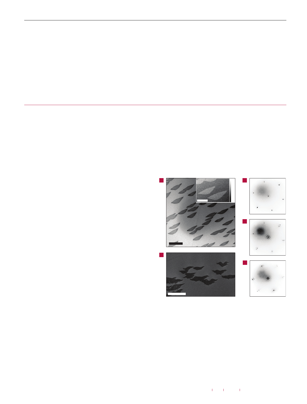
Figure 1 Morphology of epitaxial graphene on Ru(0001). a, UHV-SEM image of a
large area of the Ru(0001) surface after first-layer graphene growth. Inset: Carbon
KLL (260.6 eV) UHV scanning Auger microscopy image, obtained on this sample.
b, UHV-SEM image of a group of second-layer graphene islands. c, Selected-area
low-energy electron diffraction (electron energy: 45.4 eV) pattern of the Ru(0001)
substrate. d, Diffraction pattern of one-layer epitaxial graphene on Ru(0001)
(52.2 eV). e, Diffraction pattern of two-layer epitaxial graphene (39.1 eV).
few-layer graphene epitaxy on Ru(0001)—and possibly on other
transition-metal substrates—integrated by se lective growth on
transition-metal template pads or combined with methods for
transfer to other substrates can provide high-quality material for
applications in electronics and sensing.
406 nature materials VOL 7 MAY 2008 www.nature.com/naturematerials
© 2008 Nature Publishing Group
ARTICLES
90 s60 s30 s12 s
g
Ru
10 µm
a
b
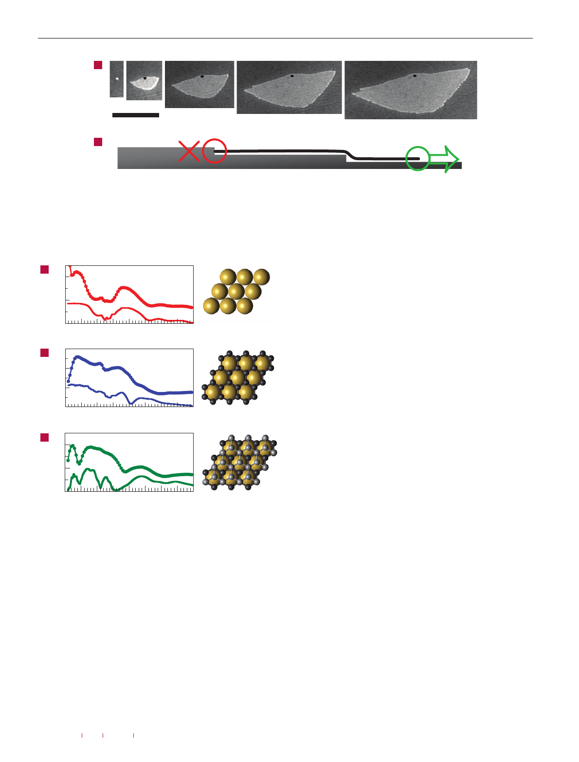
Figure 2 In situ microscopy of graphene epitaxy on Ru(0001). a, Time-lapse sequence of LEEM images showing the initial growth of a first-layer graphene island on
Ru(0001) at 850
◦
C. Numbers indica te elapsed time in seconds after the nucleation of the graphene island. Substrate steps, visible as faint dark lines, are aligned from lower
left to upper right. Black dots mark the position of the initial graphene nucleus, demonstrating negligible growth across steps in the ‘uphill’ direction. b, Schematic
cross-sectional view of the preferential, carpet-like expansion of the graphene sheet (g) across ‘downhill’ steps, and suppression of the growth in the ‘uphill’ direction.
Intensity (a.u.)
10 20 30
Energy (eV)
040
Intensity (a.u.)
10 20 30
Energy (eV)
040
Intensity (a.u.)
10 20 30
Energy (eV)
040
a
b
c
Ru
C
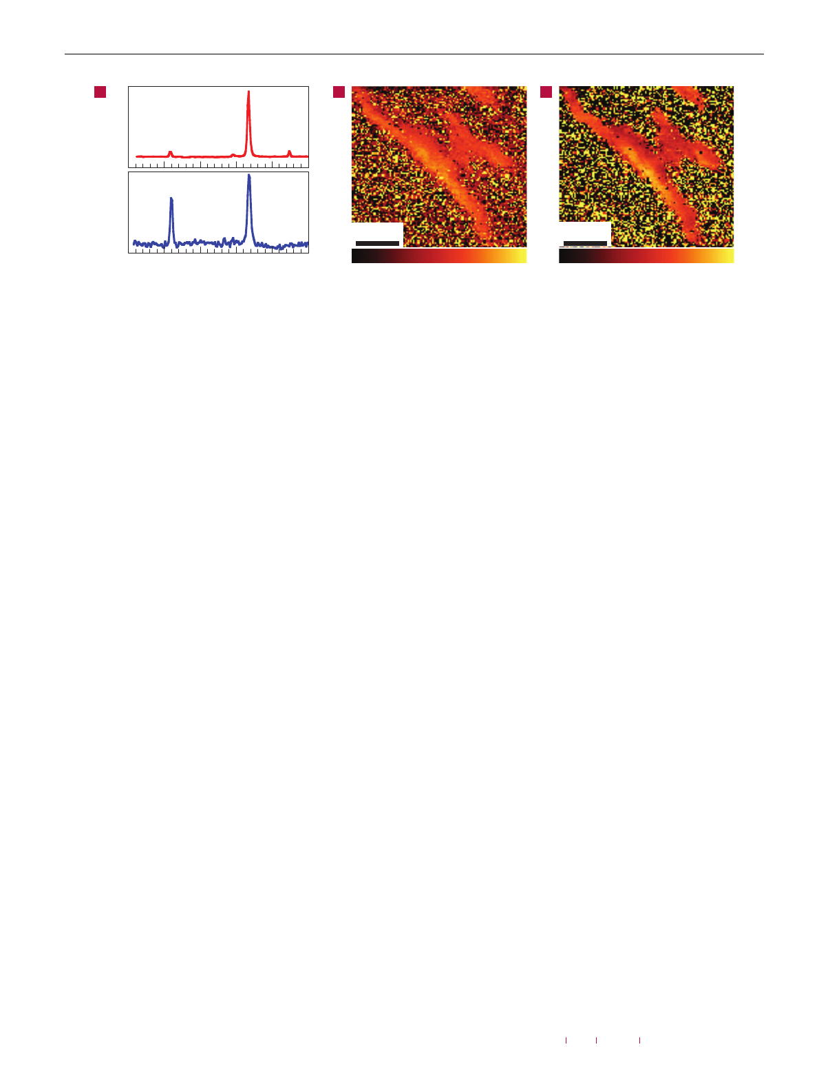
Figure 3 Identification of the layer spacing of one- and two-layer
graphene/Ru(0001). a, Measured (top) and simulated (bottom) low-energy electron
reflectivity, I (V ), of the Ru(0001) substrate. b,c, Best fit of measured and simulated
I(V ) spectra for one- and two-layer epitaxial graphene on Ru(0001). Plan-view
models of the simulated structures are shown next to the spectra.
We made use of the temperature-dependent solubility of
interstitial carbon in transition metals to achieve the controlled
layer-by-layer growth of large graphene domains on Ru(0001). At
high temperature, C is absorbed into the Ru bulk. Slow cooling
from 1,150
◦
C to 825
◦
C lowers the interstitial C solubility by a
factor of 6 (ref. 15), driving significant amounts of C to the
surface. The result is an array of lens-shaped islands of macroscopic
size (>100 µm) covering the entire Ru(0001) substrate (Fig. 1a).
Ultrahigh-vacuum (UHV) C
KLL
scanning Auger microscopy shows
that these islands are indeed C-rich, and surrounded by Ru metal
with negligible C
KLL
signal. Combining in situ electron microscopy
and selected-area electron diffraction (Fig. 1c–e), we identify these
islands as single-layer epitaxial graphene. On Ru(0001), single-layer
graphene adopts an incommensurate moir
´
e structure
11
, similar to
that observed on other transition metals, such as Ir(111) (ref. 9).
Diffraction shows that the h10
¯
10i directions of layer and substrate
align, with moir
´
e repeat vectors a
m
=(2.93 ±0.08) nm, equivalent
to 10.8±0.3 times the nearest-neighbour distance on Ru(0001). A
marked lowering of the work function compared with that of both
clean Ru and bulk graphite indicates strong substrate bonding and
significant charge transfer from the metal to the graphene overlayer.
The interaction of the growing islands with atomic substrate
steps is an important factor in enabling monocrystalline graphene
domains with size exceeding the average step spacing by several
orders of magnitude. In contrast to previous work that showed
dense nucleation at Ru step edges
11
, epitaxial graphene sheets
on Ru(0001) nucleate very sparsely and rapidly expand by
C incorporation into graphene edge sites under our growth
conditions. In situ low-energy electron microscopy (LEEM) during
growth (Fig. 2) shows a fast expansion of growing graphene
domains parallel to substrate steps and across steps in the ‘downhill’
direction. The crossing of ‘uphill’ steps by the graphene edge is
almost entirely suppressed, lea ding to a straight boundary that
shows virtually no growth. Single-layer graphene should interact
with a flat metal substrate primarily through hybridization of
the out-of-plane π orbitals with metal d bands, whereas in-plane
σ states participate in sp
2
bonding. This picture breaks down
when the graphene edge meets a substrate step. The epitaxial
orientation on Ru(0001) implies that a graphene sheet projects
a zigzag edge with localized dangling σ bonds
16
onto atomic
substrate steps. A graphene boundary encountering an ‘uphill’ step
maximizes the orbital overlap and becomes immobilized at the
step edge. Conversely, a gr aphene sheet growing in the ‘downhill’
direction shows minimal overlap of the edge states with the Ru
step, and can flow uninhibited in a car pet-like fashion across
the step
10
. T his growth mode results in macroscopic graphene
domains reaching well over 100 µm in length (Fig. 1a), far larger
than the substrate step spacing (0.15 µm), exceeding the extension
of the largest monocrystalline epitaxial graphene domains reported
so far—below 1 µm on 4H-SiC(000
¯
1) (ref. 17); about 1 µm on
Ru(0001) (ref. 12) and Ir(111) (ref. 10)—by at least two orders
of magnitude.
If sufficient C segregates from the Ru bulk (or is deposited
from a suitable hydrocarbon precursor, such as ethylene
18
), the
graphene islands grow to a size corresponding to the spacing of the
initial nuclei (>200 µm) and coalesce to a complete first layer
14
.
nature materials
VOL 7 MAY 2008 www.nature.com/naturematerials 407
© 2008 Nature Publishing Group
ARTICLES
1,586 cm
–1
2,674 cm
–1
1,599 cm
–1
2,678 cm
–1
2,620
2,720
Intensity (a.u.)
1,520
1,640
a
b
c
1,500 2,000 2,500 3,000
Raman shift (cm
–1
)
Raman shift (cm
–1
)
Raman shift (cm
–1
)
1,000 3,500
5 µm
5 µm
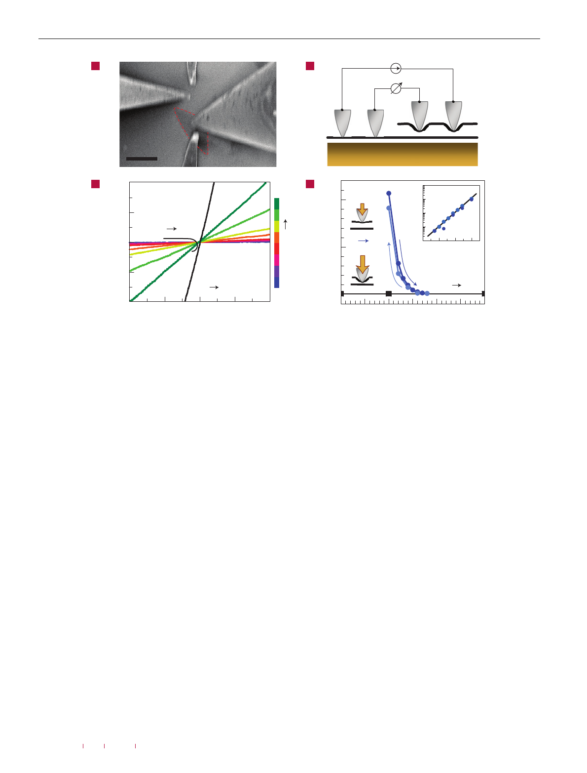
Figure 4 Micro-Raman characterization of two-layer graphene on Ru(0001). a, Comparison of Raman spectra at 532 nm for mechanically cleaved monolayer graphene
on SiO
2
(top) and epitaxial two-layer graphene on Ru(0001) (bottom). b, Raman map showing the peak energy of the G band for two adjacent two-layer epitaxial graphene
islands. c, Raman map of the peak energy of the 2D band for the same islands.
At about 80% surface coverage, the nucleation and growth of
islands of a second graphene layer are observed (Fig. 1b) on the
macroscopic first-layer domains. A smaller separation of second-
layer nuclei suggests a C adatom mobility that is lower than on
Ru(0001). A well-ordered moir
´
e structure is observed by selected-
area diffraction on the second layer (Fig. 1e). Island edges aligne d
with the direction of substrate steps indicate a residual interaction
between Ru(0001) surface steps and graphene edges, similar to that
observed for the first layer.
At this point, the surface consists of two different phases. Areas
with two-layer graphene coexist with regions covered by a single
graphene layer. We expect the first layer to be covalently bonded to
the Ru substrate by hybridization of C 2p
z
orbitals with Ru d-states
near the Fermi energy. Charge transfer from the substrate to
subsequent graphene layers should diminish progressively, with the
interlayer coupling asymptotically approaching the van der Waals
interaction of bulk graphite. Assessing this transition is of central
importance for evaluating epitaxy on transition metals as a
scalable synthesis route of one- or few-layer material with the
unique electronic properties of graphene. Going beyond the
existing surface-science studies on epitaxial graphene on Ru(0001)
(refs 10–14), we have used a combination of structural, vibrational
and electronic probes on individual single- and two-layer domains
to address this key issue.
The layer spacing has been determined by intensity–voltage
LEEM
19
, a technique capable of structural fingerprinting in
submicrometre surface areas. Spec troscopic stacks of images of
a surface were acquired from the (00) diffraction beam as a
function of electron energy, V, so that the local image intensity,
I(V ), represents the specular low-energy electron reflectivity of a
given surface domain. When combined with dynamical multiple
scattering calculations of the low-energy electron reflectivity
20
,
this information can be used to determine the spacings of our
graphene layer stacks (Fig. 3). We have applied this method to bare
Ru(0001), as well as single- and two-layer epitaxial graphene on
Ru(0001). Measured and simulated I (V ) curves are in excellent
agreement for the metal surface (Fig. 3a). On graphene, a best
fit between experimental and theoretical I(V ) curves is obtained
for a unique set of layer spacings. We determine a separat ion of
(1.45 ±0.1)
˚
A between the Ru substrate and the first graphene
layer (Fig. 3b), and a larger spacing of (3.0 ±0.1)
˚
A be tween the
first and second graphene layer in Bernal (A–B) stacking (Fig. 3c).
The addition of the second layer has negligible influence on the
separation between the first graphene layer and the metal, which
remains fixed at 1.45
˚
A. This close spacing clearly reflects the
strong bonding interaction between Ru and the first graphene
layer. Already with the second layer, however, the interlayer spacing
comes close to that of bulk graphite (3.34
˚
A), suggesting that the
electronic structure of this and further graphene layers may be
affected little by the adja cent metal substrate.
We have used Raman spectroscopy to probe the consequences
of this gr adual decoupling on the vibrational and electronic
properties of transition-metal-supported graphene stacks. R aman
spectra on cleaved monolayer and few-layer graphene on SiO
2
,
which served as reference samples, show two primary features: a
G band at ∼1,580 cm
−1
due to the two-fold degenerate E
2g
mode at
the zone centre, and a second-order D
∗
(2D) band at ∼2,700 cm
−1
due to phonons in the highest optical branch near the K point at
the Brillouin zone boundar y
21
(Fig. 4a). The 2D band results from
a double-resonance process, w hich links the phonon wave vectors
to the electronic band structure, that is, its line shape can serve as a
fingerprint of the electronic structure of massless Dirac fermions of
monolayer or few-layer graphene
21
.
Figure 4 summarizes micro-Raman experiments at 532 nm
excitation on single- and two-layer epitaxial graphene on Ru(0001).
The dominant band of the Ru substrate is the transverse-optical
zone-centre phonon mode at ∼190 cm
−1
(ref. 22). Samples with a
single epitaxial graphene layer show no detectable Raman intensity
between 1,000 and 3,000 cm
−1
. With the addition of the second
graphene layer, peaks appear at frequencies close to those of the
G and 2D bands (Fig. 4a). Both bands give rise to narrow single
peaks, which are shifted to hig her energy by 13 cm
−1
and 4 cm
−1
,
respectively, compared with the same bands in mechanically cleaved
monolayer graphene. In Raman maps, the centre position and
width of these bands remain constant over large areas within
two-layer epitaxial graphene domains several square micrometres
in size (Fig. 4b,c). A local blueshift by ∼10 cm
−1
is detected in a
continuous area within one of the sampled islands.
The double-resonance process that gives rise to the 2D band
has been used to distinguish monolayer and two-layer graphene
21
.
For cleaved g raphene, the 2D band is defined largely by the
dispersion and splitting of electronic bands at the Brillouin zone
boundary: a single peak is observed for monolayer graphene,
whereas interlayer coupling splits the band into four distinct
components for bilayer graphene. The 2D band of two-layer
epitaxial graphene on Ru(0001) shows a single peak that is
broadened (full-width at half-maximum 42 cm
−1
) with respect to
that of monolayer graphene on SiO
2
(full-width at half-maximum
408 nature materials VOL 7 MAY 2008 www.nature.com/naturematerials
© 2008 Nature Publishing Group
ARTICLES
Resistance (kΩ)
Ru
G
1
G
1
G
1
G
2
G
1
G
2
12
34
I
V
10
10 μm
1
2
3
4
G
1
G
2
Compression
G
1
G
2
G
1
G
1
–1 0 1
Voltage V
2,3
(mV)
–2 2
0
–20
20
I
1,4
(μA)
–40
40
5
10
0
12
Probe height (a.u.)
03
Separation (Å)
1203
10
2
10
3
10
4
Resistance (Ω)
10
1
10
5
a
b
c
d
Figure 5 Measurement of interlayer electrical transport. a, UHV-SEM image of the arrangement of four contact probes for interlayer resistance measurement.
b, Schematic diagram of the four-probe transport measurement between first- and second-layer epitaxial graphene (G
2
→G
1
), using probes 1 and 2 for local mechanical
deformation of G
2
. c, Four-probe current–voltage characteristics for G
1
→G
1
transport, and for G
2
→G
1
transport at different compression of the interlayer spacing.
d, Comparison of the strain dependence of the electrical resistance in G
1
→G
1
(black squares) and G
2
→G
1
(blue circles) transport. Dark and light blue curves correspond to
mechanical loading and unloading, respectively. Inset: Exponential scaling of interlayer resistance with calculated layer spacing.
38 cm
−1
). The observ ation of a single narrow peak suggests that our
two-layer samples closely match the electronic str ucture of cleaved
monolayer graphene, with very little observable band splitting due
to interaction of the second layer with the underlying graphene
layer and Ru metal. Hence, the controlled a ddition of further
epitaxial graphene layers could be used to realize the properties of
bilayer and few-layer graphene.
The frequencies and intensity ratios of the G and 2D
peaks observed for two-layer graphene on Ru(0001) (Fig. 4a) are
consistent with results obtained on cleaved graphene, the carrier
density of which is increased by a gate-induced electric field
23–25
,
suggesting that the Fermi level in the epitaxial two-layer graphene
is shifted away from the Dirac point. Chemical doping—reflecting
a residual interac tion with the underlying metal, indicated by the
spacing of the first and second graphene layers and varying slightly
across the graphene sheets (Fig. 4b,c)—is the most likely cause.
Both the structural data from intensity–voltage LEEM and
the coupled vibrational and electronic signatures in Raman
spectroscopy indicate that the se cond-layer epitaxial graphene
on Ru(0001) is strongly decoupled from the metal substrate.
This decoupling should also be reflected in the interlayer
electronic transport. To evaluate carrier transport through epitaxial
graphene stacks, we have carried out room-temperature four-
probe transport measurements in UHV, using an instrument
that enables the controlled positioning of probes on the sample
surface under a field-emission scanning electron microscope
(Fig. 5a). Measurements were carried out for two different probe
configurations: G
2
→G
1
, two probes each on the first and second
graphene layer for measuring transport between graphene sheets;
and G
1
→G
1
, all four probes on the first graphene layer.
At identical probe spacing, the measured intralayer and
interlayer resistances differ significantly. For voltage probes (2,3)
separated by about 10 µm (Fig. 5a), transport in the first graphene
layer (G
1
→ G
1
) shows a resistance of (10 ±1) . The interlayer
resistance (G
2
→ G
1
) is higher by about a factor of 10
3
, that is,
the electronic coupling between the graphene layers—and hence
between the second graphene sheet and the Ru substrate—is weak.
The electronic interaction between sheets with exposed π
orbitals is important in a variety of contexts. It determines
the anisotropy between the in-plane and c-axis conductance of
bulk graphite
26
, affects electronic transport in multiwall carbon
nanotubes
27,28
and nanotube bundles
29
and governs charge transfer
in junctions containing π-conjugated molecules
30
. Depending on
the alignment of adjacent layers, the interlayer transport involves
either hopping or tunnelling between adjacent π orbitals. T he
coupling mechanism can, in principle, be identified by measuring
the interlayer resistance as a function of layer spacing. Early
experiments on graphite subje cted to high hydrostatic pressures
indeed showed a lowering of the c-axis resistance at high pressure
31
.
A similar type of measurement can be realized on individual
micrometre-sized graphene domains using our nanomanipulated
electrical probes (Fig. 5b–d). With probes 3 and 4 placed on G
1
,
probes 1 and 2—in contact with G
2
—are moved along the sample
normal to deform G
2
. The relative stiffness of the tungsten probe tip
and the graphene layer generates a large mechanical advantage, n,
in the range 10
2
–10
3
, that is, a sub-angstrom deformation of G
2
can
be induced controllably by an n-fold larger displacement of the tip
actuator. Measurements during loading and subsequent unloading
coincide exactly, demonstrating that the graphene sheet is strained
elastically in this process. Reference measurements with all four
nature materials
VOL 7 MAY 2008 www.nature.com/naturematerials 409
© 2008 Nature Publishing Group

ARTICLES
probes placed on G
1
showed no change in electrical characteristics
over a much larger range of loading.
Figure 5c,d shows the four-probe resistance as a funct ion of the
spacing between G
2
and G
1
. For low bias voltages (few millivolts),
all measured current–voltage characteristics, I
1,4
(V
2,3
), are linear.
The interlayer resistance varies exponentially with the deformation
of G
2
, from which we identify direct tunnelling between π-orbitals
on the adjacent graphene sheets as the conduction mechanism.
We fit the measured resistance to a one-dimensional tunnelling
model
30
, I ∝ V exp(−2d
√
2m
e
φ/
¯
h), where d and φ are the
width and constant height (at low V) of the tunnelling barrier,
respectively, and m
e
denotes the electron (effective) mass. Assuming
m
e
= m
0
, we find a barrier height of 5.0 eV, consistent with very
weak electronic interlayer coupling of the undeformed graphene
stack at room temperature.
Our experiments on a specific model system—single- and two-
layer graphene grown epitaxially on a Ru(0001) template—provide
evidence for the feasibility of synthesizing large monocr ystalline
epitaxial graphene domains. A comparison with graphene on
SiC, the epitaxial system that has received most attention so far,
shows surprisingly similar substrate interactions in both cases: a
first graphene layer is spaced closely (1.45
˚
A for Ru; 1.65
˚
A for
4H-SiC(000
¯
1) (ref. 32)) and interacts strongly with the substrate,
as reflected by a drastic suppression of the work function
33
. This
layer, which will have distinct electronic and chemical properties
that are yet to be explored, may be seen as a buffer layer supporting
the second graphene sheet that is largely decoupled structurally and
electronically, but is doped owing to residual charge t ransfer from
the substrate
8
. Significant differences between graphene epitaxy
on Ru(0001) and SiC clearly lie in the process conditions and
in the level of structural control achievable. Si sublimation on
SiC at high temperatures (between 1,250 and 1,450
◦
C) apparently
leads to small (<1 µm) multilayer graphene nuclei. Epitaxy on
Ru(0001) at lower temperatures (∼850
◦
C) produces sparse arrays
of graphene nuclei that grow in a controlled layer-by-layer mode to
macroscopic dimensions.
Our findings open up a number of avenues for exploiting
graphene epitaxy on transition-metal templates. The large first-
layer graphene domains could be isolated if etch processes are found
that selectively remove the Ru substrate but do not damage the
graphene layer
1
. It can be predicted that the weakly bound second
graphene layer be transferred to another substrate, for example,
using intercalation to further weaken the interlayer bonding
34
,
analogous to the layer transfer methods used successfully for
other e lectronic materials, such as Ge and strained Si (ref. 35). A
perhaps more intriguing possibility is the integration with other
materials by using lithographically patterned transition-metal pads
as a catalyst and template for directed local graphene growth.
A similar seeding approach using catalytic Au nanoparticles has
been established recently to assemble highly ordered few-layer
graphene sheets conformally on semiconductor (Ge (ref. 36), GaN
(ref. 37)) nanowires. Finally, our demonstration of an atomic-layer
switch, the out-of-plane conductance of which is reversibly altered
over three orders of magnitude by tuning the graphene-substrate
coupling, suggests the possibility of controlling the in-plane carrier
transport in epitaxial or cleaved bilayer or few-layer graphene by
‘mechanical gating’, that is, local mechanical deformations of the
layer stack.
METHODS
GRAPHENE GROWTH AND STRUCTURAL ANALYSIS
Graphene growth was carried out by thermal cycling of a Ru(0001) single crystal
in UHV, as described in the text, while observing the process by in situ LEEM.
Time-lapse LEEM movies were obtained during growth of the first and second
epitaxial graphene layer. Selected-area low-energy electron diffraction was
carried out on micrometre-sized areas of the bare Ru substrate, as well as the
first and second graphene layer. Local intensity–voltage (I(V )) characteristics
were obtained from real-space images of uniform Ru metal, one-layer and
two-layer g raphene, acquired as a function of incident electron energy. Layer
spacings were determined by comparing measured I (V ) characteristics for
the specular diffrac ted beam at very low electron energies (1–40 eV) with
simulations by dynamical multiple-scattering low-energy electron diffraction
theory
20
. As an approximation to the incommensurate moir
´
e structure
observed experimentally, the simulations assumed graphene fully strained
to the Ru substrate, with C atoms occupying hexagonal close-packed and
face-centred-cubic hollow sites. We thus achieved a faithful representation of
the out-of-plane layer separations at reasonable computational efficiency.
MICRO-RAMAN SPECTROSCOPY AND MICROSCOPY
Micro-Raman spectra and Raman maps were obtained on both epitaxial
graphene on Ru(0001) and on a reference sample of mechanically cleaved
monolayer graphene in a commercial confocal R aman microscope (WiTec).
We used an excitation wavelength of 532 nm at incident power below 1 mW,
and a ×100 objective providing a diffraction-limited spot size of about 400 nm.
Raman maps were acquired by measuring complete spectra on a 0.5 µm grid
over a 25 µm×25 µm sample area. Figure 4b,c was obtained by lorentzian fits to
the G and 2D Raman bands, and plotting the spatial distribution of the Raman
shifts of these bands.
TRANSPORT MEASUREMENTS
Electrical transport measurements were carried out in UHV in a commercial
system (Omicron Nanotechnology) that enables positioning of four
independent probe tips with nanometre accuracy on the sample while
observing the process by field-emission scanning electron microscopy (SEM).
The probes consisted of electrochemically sharpened tungsten wires mounted
on and manipulated by piezoelectric actuator elements, and projecting under
45
◦
onto the sample surface. Their tips were placed above selected epitaxial
graphene structures, biased relative to the sample, and then approached
individually until a tunnelling current was detected. From this tunnelling
contact, the tips were carefully brought into mechanical contact, as judged
from the onset of linear low-bias four-probe current–voltage char acteristics.
A controlled compression of the graphene layer G
2
and measurement of the
resulting change in interlayer electrical resistance was achieved by driving
one of the probes on G
2
closer to the sample using a piezoelectric actuator
while measuring both the displacement of the actuator and the four-probe
resistance between G
1
and G
2
. The different stiffnesses of the probe wire
(10 mm long, 0.25 mm diameter) and of the graphene sheet G
2
converted large
(several hundred
˚
angstr
¨
oms) movements of the actuator into much smaller
deformations of G
2
. The resulting reduction of the separation between G
1
and
G
2
(Fig. 5d, inset) was inferred from three measured quantities: (1) the relaxed
interlayer spacing, d
0
(G
1
,G
2
) =3.0
˚
A, determined by e lectron diffraction;
(2) the interlayer resistance between the undeformed graphene layer G
2
and the
underlying layer G
1
(10 k at d
0
(G
1
,G
2
) =3.0
˚
A); and (3) the resistance for
G
1
→G
1
transport, assumed equal to the resistance between G
1
and G
2
at zero
spacing (10 at d(G
1
,G
2
) =0). Using the interlayer resistances at 3.0
˚
A and
zero spacing as known end points, an exponential fit to the measured resistance
as a function of actuator position provided the conversion between actuator
elongation and deformation of G
2
, assuming that the two are proportional to
each other (that is, differ by a constant factor). All four-probe current–voltage
curves were measured with the sample held at room temperature, using a
programmable semiconductor test system (Keithley, model 4200SCS).
Received 16 November 2007; accepted 12 March 2008; published 6 April 2008.
References
1. Geim, A. K. & Novoselov, K. S. The rise of graphene. Nature Mater. 6, 183–191 (2007).
2. Novoselov, K. S. et al. Two-dimensional gas of massless Dirac fermions in graphene. Nature 438,
197–200 (2005).
3. Bostwick, A. et al. Quasiparticle dynamics in graphene. Nature Phys. 3, 36–40 (2007).
4. Novoselov, K. S. et al. Electric field effect in atomically thin carbon films. Science 306, 666–669 (2004).
5. Berger, C. et al. Electronic confinement and coherence in patterned epitaxial graphene. Science 312,
1191–1196 (2006).
6. Chen, Z., Lin, Y.-M., Rooks, M. J. & Avouris, P. Graphene nano-ribbon electronics. Physica E 40,
228–232 (2007).
7. Schedin, F. et al. Detection of individual gas molecules adsorbed on graphene. Nature Mater. 6,
652–655 (2007).
8. de Heer, W. A. et al. Epitaxial graphene. Solid State Commun. 143, 92–100 (2007).
9. N’Diaye, A. T., Bleikamp, S., Feibelman, P. J. & Michely, T. Two-dimensional Ir cluster lattice on a
graphene moire on Ir(111). Phys. Rev. Lett. 97, 215501 (2006).
410 nature materials VOL 7 MAY 2008 www.nature.com/naturematerials
© 2008 Nature Publishing Group

ARTICLES
10. Coraux, J., N’Diaye, A. T., Busse, C. & Michely, T. Structural coherency of graphene on Ir(111). Nano
Lett. 8, 565–570 (2008).
11. Marchini, S., Gunther, S. & Wintterlin, J. Scanning tunneling microscopy of graphene on Ru(0001).
Phys. Rev. B 76, 075429 (2007).
12. Vazquez de Parga, A. L. et al. Periodically rippled graphene: Growth and spatially resolved electronic
structure. Phys. Rev. Lett. 100, 056807 (2008).
13. Pan, Y., Shi, D.-X. & Gao, H.-J. Formation of graphene on Ru(0001) surface. Chinese Phys.
3151 (2007).
14. Pan, Y. et al. Millimeter-scale, hig hly ordered single crystalline graphene grown on Ru (0001) surface.
Preprint at <http://arxiv.org/abs/0709.2858> (2007).
15. Arnoult, W. J. & McLellan, R. B. The solubility of carbon in rhodium, ruthenium, iridium, and
rhenium. Scr. Metall. 6, 1013–1018 (1972).
16. Nakada, K., Fujita, M., Dresselhaus, G. & Dresselhaus, M. S. Edge state in graphene ribbons:
Nanometer size effect and edge shape dependence. Phys. Rev. B 54, 17954 (1996).
17. Hass, J. et al. Highly ordered graphene for two dimensional e lectronics. Appl. Phys. Lett. 89,
143106 (2006).
18. Land, T. A. et al. STM investigation of single layer graphite structures produced on Pt(111) by
hydrocarbon decomposition. Surf. Sci. 264, 261–270 (1992).
19. Schmid, A. K. et al. The chemistry of reaction-diffusion fronts investigated by microscopic LEED I–V
fingerprinting. Surf. Sci. Part 1 331–333, 225–230 (1995).
20. Blum, V. & Heinz, K. Fast LEED intensity calculations for surface crystallography using tensor LEED.
Comput. Phys. Commun. 134, 392–425 (2001).
21. Ferrari, A. C. et al. Raman spectrum of graphene and graphene layers. Phys. Re v. Lett. 97,
187401–187404 (2006).
22. Olijnyk, H., Jephcoat, A. P. & Refson, K. On optical phonons and elasticity in the hcp transition
metals Fe, Ru and Re at high pressure. Europhys. Lett. 53, 504–510 (2001).
23. Yan, J., Zhang, Y., Kim, P. & Pinczuk, A. Electric field effect tuning of electron–phonon coupling in
graphene. Phys. Rev. Lett. 98, 166802–166804 (2007).
24. Pisana, S. et al. Breakdown of the adiabatic Born–Oppenheimer approximation in graphene. Nature
Mater. 6, 198–201 (2007).
25. Das, A. et al. Electrochemically top gated graphene: Monitoring dopants by Raman scattering.
Preprint at <http://arxiv.org/abs/0709.1174> (2007).
26. Matsubara, K., Sugihara, K. & Tsuzuku, T. Electrical resistance in the c direction of graphite. Phys.
Rev. B 41, 969 (1990).
27. Bachtold, A. et al. Aharonov–Bohm oscillations in carbon nanotubes. Nature 397, 673–675 (1999).
28. Bourlon, B. et al. Determination of the intershell conductance in multiwalled carbon nanotubes.
Phys. Rev. Lett. 93, 176806 (2004).
29. Bockrath, M. et al. Single-electron transport in ropes of carbon nanotubes. Science 275,
1922–1925 (1997).
30. Beebe, J. M. et al. Transition from direct tunneling to field emission in metal–molecule–metal
junctions. Phys. Rev. Lett. 97, 026801–026804 (2006).
31. Drickamer, H. G. Pi electron systems at high pressure. Science 156, 1712 (1967).
32. Varchon, F. et al. Electronic structure of epitaxial gr aphene layers on SiC: Effect of the substrate. Phys.
Rev. Lett. 99, 126805 (2007).
33. Mattausch, A. & Pankratov, O. Ab initio study of graphene on SiC. Phys. Rev. Lett. 99,
076802–076804 (2007).
34. Dresselhaus, M. S. & Dresselhaus, G. Intercalation compounds of graphite. Adv. Phys. 51,
1–186 (2002).
35. Maleville, C. & Mazure, C. Smart-cut technology: From 300 mm ultrathin SOI production to
advanced eng ineered substrates. Solid State Electron. 48, 1055–1063 (2004).
36. Sutter, P. W. & Sutter, E. A. Dispensing and surface-induced crystallization of zeptolitre liquid
metal-alloy drops. Nature Mater. 6, 363–366 (2007).
37. Sutter, E. et al. Assembly of ordered carbon shells on GaN nanowires. Appl. Phys. Lett. 90,
093118 (2007).
Acknowledgements
The authors thank T. Valla and J. Camacho for access to a cleaved monolayer graphene
sample. Work carried out under the auspices of the US Department of Energy under contract
No. DE-AC02-98CH1-886.
Author contributions
P.W.S. and E.A.S. planned the study, carried out all experiments, and analysed the data. J.-I.F. carried
out the LEED I(V ) simulations. P.W.S. wrote the paper, and all authors commented on the manuscript.
Author information
Reprints and permission information is available online at http://npg.nature.com/reprintsandpermissions.
Correspondence and requests for materials should be addressed to P.W.S.
nature materials
VOL 7 MAY 2008 www.nature.com/naturematerials 411
© 2008 Nature Publishing Group
