June 2012
11
physicsworld.com
Applications
Physics World Focus on: Nanotechnology
20 things you can do with graphene
Graphene – a sheet of carbon atoms
arranged in a honeycomb-like lattice just
one atom thick – has trumped buckyballs
and nanotubes to become the king of car-
bon nanomaterials. Since its discovery just
a few years ago, this “wonder material” has
wowed researchers with record-breaking
electronic and mechanical properties.
According to recent studies, graphene is not
only the strongest material ever measured,
but also the stiffest, and its current density
– a measure of the density of flow of charged
carrier particles – is a million times that of
copper. But graphene is much more than
just a scientific curiosity: it boasts a growing
list of real-world applications. To illustrate
the point, here are 20 amazing things that
you can do with it.
Create rugged sensors
Two-dimensional graphene is very stable
electrically and mechanically under high
bending deformation, and combining it with
vertically aligned metallic nanowires offers
a promising way of making flexible hybrid
nanostructures. Applications include bio-
chemical sensors, pressure sensors, field
emission devices and battery electrodes
(Nanotechnology 22 355709).
Researchers from Seoul National Univer-
sity and the Samsung Advanced Institute of
Technology in South Korea have developed
a simple, but efficient, low- temperature pro-
duction route. In the method, a graphene
layer is transferred onto an anodic alumina-
oxide template and vertically aligned gold
nanowires are grown on the graphene sur-
face via electrodeposition, which allows the
structures to be prepared with a controlled
length and diameter.
The technique also avoids any high-
temperature steps or unconventional
lithography procedures, which means that
it can be applied onto versatile substrates
including soft materials.
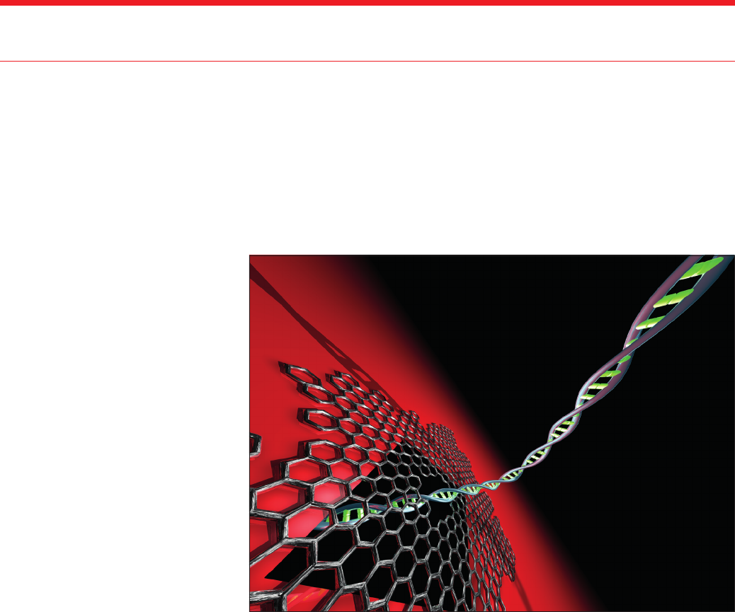
Sequence DNA
By feeding individual strands of DNA
through nanometre-sized holes, scientists
from Delft University of Technology in
the Netherlands say that they have proved
the principle of a revolutionary DNA-
sequencing technique. The breakthrough is
part of a worldwide race to develop fast and
low-cost strategies to analyse these codes
that underpin the chemistry of life (Nano.
Lett. 10.1021/nl102069z).
In the study, the team demonstrates
that DNA does indeed go through little
holes in graphene, and that it does so with
great speed. Both of these are important
advancements towards using graphene for
DNA sequencing.
Re-imagine aircraft design
Picture a deep-space-exploration vehi-
cle fitted out with lightweight actuators
that directly convert photons from nearby
stars into mechanical motion without
the need for solar cells. Or how about an
aircraft equipped with solid-state flight-
control surfaces instead of rudders and
ailerons? These ideas might sound a little
like science fiction, but researchers in the
US and the UK are developing graphene
nanoplatelet-based photomechanical actu-
ators that could pave the way for both con-
cepts (Nanotechnology 23 045501).
By combining graphene with soft elas-
tomeric materials such as PDMS, the sci-
entists from the University of Louisville
and the University of Cambridge have cre-
ated graphene/polymer composites with
responses to near-infrared illumination
that depend on applied pre-strain. At low
levels of pre-strains (3–9%) the actuators
show reversible expansion, while at high
levels (15–40%) the actuators exhibit
reversible contraction. Using these actua-
tors, the team witnessed an extraordinary
optical-to-mechanical energy conversion
factor of ~7 MPa/W, some three orders of
magnitude greater than commercially avail-
able light-driven actuating materials such as
polyvinylidene fluoride.
Detect concealed weapons
Scientists at the Lawrence Berkeley
National Laboratory and the University of
California, Berkeley in the US have found
a way to adjust the amount of light absorbed
by graphene at terahertz frequencies. The
findings could lead to graphene-based
terahertz metamaterials, which would
give developers more options for applica-
Dubbed the “wonder material”, graphene has grabbed the attention of developers worldwide thanks to
its extraordinary properties and diverse range of uses. Belle Dumé and James Tyrrell round up
20 exciting applications that have hit the headlines
Code breaker Researchers have shown that DNA can go t hrough tiny hole s in gr aphene.
Cees Dekke r L ab T U Delft /Tremani
PWNANOJun12Graphene.indd 11 15/05/2012 10:15

12
June 2012
physicsworld.com
Applications
Physics World Focus on: Nanotechnology
tions such as medical imaging and security
screening (Nature Nanotechnology 10.1038/
nnano.2011.146).
Terahertz radiation is useful for detect-
ing items such as concealed weapons and
explosives because it passes through cloth-
ing and packaging but is strongly absorbed
by metals and other inorganic substances.
Feng Wang and colleagues say that they
have made the “beginnings of a toolset” for
experiments in this wavelength range. The
team has come up with a prototype device
that consists of an array of graphene nano-
ribbons with a response to terahertz radia-
tion that can be tuned by varying the width
of the ribbons and the number of charge car-
riers (electrons and holes) in the structures.
In graphene, the concentration of charge
carriers can easily be increased or decreased
by applying a strong electric field – a tech-
nique known as electrostatic doping.
Build better electronics
Graphene could be ideal for use in future
electronics applications because electrons
whizz through the material at extremely
high speeds (thanks to the fact that they
behave like relativistic particles with no rest
mass). Recently, a new method to increase
the amount of current that can be carried
by graphene has been unveiled by research-
ers at the University of California, River-
side (UCR) and the Argonne National Lab
(Nano Lett. 10.1021/nl204545q).
The technique involves growing or trans-
ferring graphene on synthetic diamond or
ultrananocrystalline diamond rather than
on a conventional silicon-dioxide substrate.
Diamond conducts heat better than silicon
or silicon dioxide, removing more heat away
from the graphene, which in turn means
that the wonder material can sustain even
higher current densities.
Alexander Balandin and Anirudha
Sumant, working together with electrical-
engineering graduate students in Bal-
andin’s lab at UCR, have shown that the
current-carrying capacity of graphene
can be increased to as high as around
20 µA/nm
2
by replacing the silicon diox-
ide with synthetic diamond or inexpensive
ultrananocrystalline diamond.
The work could help to develop high-
frequency transistors, transparent elec-
trodes and interconnects for replacing
copper on silicon dioxide.
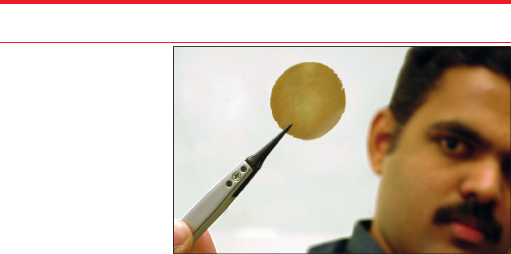
Ramp up the performance of
supercapacitors and batteries
A new and simple “dipping” technique
that significantly improves the specific
capacitance and rate capability of metal-
oxide-based supercapacitors has been
demonstrated by researchers at Stanford
University in the US (Nano Lett. 10.1021/
nl2026635).
The technique, developed by Zhenan
Bao, Yi Cui and colleagues, involves dip-
ping a composite electrode made of gra-
phene/manganese-oxide into a solution
containing either carbon nanotubes (CNTs)
or a conductive polymer. The CNTs or poly-
mer coat the electrode and greatly improve
its electrical conductivity, so enhancing its
specific capacitance (or its ability to store
charge) by more than 20% for the CNT
coating and 45% for the polymer.
Dubbed “conductive wrapping”, the
method could be applied to a range of
high-density but insulating electrode mate-
rials. It may even be used to improve next-
generation lithium-ion battery electrodes
made from sulphur, lithium manganese
phosphate and silicon.
As well as having high specific capacitance,
the hybrid electrodes also show good rate
capability. They can be used over more than
3000 charge–discharge cycles while retain-
ing more than 95% of their capacitance.
Design new types of batteries
Researchers at Hong Kong Polytechnic
University claim to have invented a new
kind of graphene-based “battery” that
runs solely on ambient heat. The device
is said to capture the thermal energy of
ions in a solution and convert it into elec-
tricity. The results are in the process of
being peer reviewed, but, if confirmed,
such a device might find use in a range of
applications, including powering artificial
organs from body heat, generating renew-
able energy and running electronic devices
(arXiv:1203.0161).
Zihan Xu and colleagues made their bat-
tery by attaching silver and gold electrodes
to a strip of graphene. In their experiments,
the researchers showed that six of these
devices in series placed in a solution of
copper-chloride ions produced a voltage of
more than 2 V – enough to drive a commer-
cial red light-emitting diode.
Kill E . coli
Graphene could be used to make antibacte-
rial paper, according to work by scientists at
the Chinese Academy of Sciences in Shang-
hai, who have found that sheets of the mate-
rial effectively stop the growth of E. coli
bacteria without being toxic to human cells.
“Ultimately, we would like to develop new
antibacterial materials from graphene that
could be directly applied onto skin to aid
in wound healing,” says Chunhai Fan (ACS
Nano 10.1021/nn101097v).
Print electronic devices
Researchers at the University of Cambridge
in the UK have invented a new ink based
on graphene, which they have used to print
high- performance, transparent, thin-film
transistors and interconnects. The work
could lead to graphene-based flexible
displays, solar cells and electronic paper
(arXiv:1111.4970).
To make the ink, the scientists begin by
treating graphite flakes in a sonic bath con-
taining the solvent N-methylpyrrolidone
for several hours. The flakes are then left
to settle for a few minutes after sonication.
Next, the team decants the dispersions and
centrifuges the samples for an hour to filter
out any flakes bigger than 1 µm across that
might clog the printer nozzle.
The ink suits a variety of substrates,
including silicon dioxide and quartz.
Soak up arsenic
A composite material made from reduced
graphene oxide (RGO) and magnetite could
effectively remove arsenic from drinking
water, according to work done in South
Korea (ACS Nano 10.1021/nn1008897).
The purification process is initiated by
dispersing the magnetite–RGO composite
in water, where the material soaks up arse-
nic. Thanks to the presence of the mag-
netite, the composite can be quickly and
efficiently extracted from the water using a
permanent magnet.
The contribution of the graphene
flakes is to increase the number of arsenic
adsorption sites.
Improve electron sources
Few-layer graphene (FLG) has exceptional
physical and chemical properties and is con-
sidered as a type of field-emission material
thanks to its thin edges. However, to achieve
a large field-enhancement factor, the gra-
phene sheets must be grown vertical to the
substrate rather than in the horizontal con-
figuration that is typical of most synthesis
methods (Nanotechnology 23 015202).
One approach, as demonstrated by scien-
tists in China, is to use microwave plasma-
enhanced chemical vapour deposition
(MPECVD). The team from Sun Yat-sen
University has synthesized FLG in a vertical
growth direction, and shaped the material by
adjusting the growth time and ratio of hydro-
carbon gas. Potential applications include
high-power vacuum electron sources.
High-performance coating Graphene/manganese
elec trodes dipped into a car bon - nanotube solution.
G Yu, St anford Universi ty
PWNANOJun12Graphene.indd 12 15/05/2012 10:15
June 2012
13
physicsworld.com
Applications
Physics World Focus on: Nanotechnology
Focus light
A tiny bubble of graphene could be used
to make an optical lens with an adjustable
focal length. That is the claim of physicists
at the University of Manchester in the UK,
who have shown that the curvature of such
bubbles can be controlled by applying an
external voltage. Devices based on the dis-
covery could find use in adaptive-focus sys-
tems that try to mimic how the human eye
works (Appl. Phys. Lett. 99 093103).
It turns out that graphene can be stretched
by up to 20%, which means that bubbles of
various shapes can be “blown” from the
material. This property, combined with the
fact that graphene is transparent to light
yet impermeable to most liquids and gases,
could make the material ideal for creating
adaptive-focus optical lenses.
Such lenses are used in mobile-phone
cameras, webcams and auto-focusing eye
glasses, and are usually made of transpar-
ent liquid crystals or fluids. Although such
devices work well, they are relatively dif-
ficult and expensive to make. In principle,
graphene-based adaptive optics could be
fabricated using much simpler methods
than those used for existing devices. They
could also become cheaper to produce if
industrial-scale processes to manufacture
graphene devices become available.
Make high-performance modulators
A modulator containing a double layer of
graphene has been unveiled by researchers
at the University of California, Berkeley
and the Lawrence Berkeley National Labo-
ratory in the US. The high-performance
device, which operates at 1 GHz, has many
advantages over silicon photonics, includ-
ing a small footprint, low power consump-
tion and low optical loss. Applications
include telecommunications and on-chip
data communication (Nano Lett. 10.1021/
nl204202k).
“Compared with silicon-based optical
modulators, this double-layer graphene
device has separate electrical and optical
control modules,” says team member Ming
Liu. “This is a first and allows us to opti-
mize both the electrical and optical design
separately, and avoid the trade-off between
speed and optical losses.”
Store hydrogen
Vehicles and other systems powered by
hydrogen have the advantage of emitting
only water as a waste product. An impor-
tant challenge, however, is storing enough
hydrogen onboard a car so that it can travel
as far as a vehicle powered by fossil fuels. If
hydrogen is stored as a compressed gas, it
takes up far too much space – and liquefying
hydrogen is expensive in terms of both cost
and energy.
One solution to this problem is to exploit
the fact that many solid materials will
absorb large amounts of hydrogen, and
researchers have identified stacked layers
of oxidized graphene as a promising can-
didate. Scientists from the NIST Center
for Neutron Research in the US have made
graphene-oxide frameworks that can hold
roughly 1% of their weight in hydrogen.
This value is 100 times more than graphene
oxide and compares well with MOF-5 (the
most studied metal-organic framework to
date for hydrogen storage), which absorbs
about 1.3 wt% (Angew. Chem. Int. Ed. Engl.
49 8902).
Remove water from a mixture
Scientists have reported that membranes
made from graphene oxide appear to be
highly permeable to water while being
impermeable to all other liquids and
gases. The membranes consist of millions
of small flakes of graphene oxide with
nanometre-sized empty channels (or cap-
illaries) between the flakes that favour
the passage of monolayers of water and
resist other substances (Science 335 442).
Graphene oxide is similar to ordinary gra-
phene but is covered with molecules, such as
hydroxyl groups (OH).
Remove unwanted heat from electronics
University of California, Riverside scien-
tists say that they have made a new thermal
interface material (TIM) that could effi-
ciently remove unwanted heat from elec-
tronic components such as computer chips
and light-emitting diodes. The material is a
composite made of graphene and multilayer
graphene (Nano Lett. 10.1021/nl203906r).
Unwanted heat is a big problem in mod-
ern electronics based on conventional sili-
con circuits – and the issue is getting worse
as devices become ever smaller and more
sophisticated. Graphene could be ideal as
a filler material in TIMs to carry away heat
because pure graphene has a large intrinsic
room- temperature thermal conductivity
that lies in the 2000–5000 W m
–1
K
–1
range.
These values are higher than those of dia-
mond, the best bulk-crystal heat conductor
that is known.
Alexander Balandin and colleagues
have now succeeded in increasing the ther-
mal conductivity of a routinely employed
industrial epoxy-resin-based TIM, or
“grease” as it is better known in the indus-
try, from around 5.8 W m
–1
K
–1
to a record
14 W m
–1
K
–1
. The filler particles in this
case consist of an optimized mixture of
graphene and few-layer graphene, with the
volume fraction of the carbon-based mate-
rial in the epoxy being very low at just 2%.
Form transparent electrodes for displays
Tae-Woo Lee of Pohang University of Sci-
ence and Technology in South Korea and
colleagues have developed a way to increase
the work function of graphene films and
lower the sheet resistance so that the
ultrathin material can be made into an effi-
cient anode for organic light-emitting diode
applications (Nature Photonics 10.1038/
nphoton.2011.318).
“The graphene anode demonstrated
excellent bending stability with a bending
radius of 0.75 cm and a strain of 1.25%,”
says Lee. “And we observed that the gra-
phene devices maintained almost the same
current density even after being bent and
straightened 1000 times.”
Make rare-element-free magnets
Graphene can be made magnetic by form-
ing honeycomb-like arrays of hydrogen-ter-
minated nanopores on it. So say researchers
in Japan, based at Aoyama Gakuin Uni-
Magic membranes Flakes of graphene oxide could be used to separate water from other liquids.
University of Manchester
PWNANOJun12Graphene.indd 13 15/05/2012 10:16

physicsworld.com
Applications
Physics World Focus on: Nanotechnology
Hannover, Germany info@particular.e u particular.eu
Particular GmbH
PARTICULAR
®
NANO-GOLD
FACILE STAINING,
LABELING, TAGGING!
direct conjugation to your
biomolecules in our labs:
Î no photobleaching
Î brighter than dyes
Î visible in histology and
electron microscopy
made by physical
laser ablation:
Î pure, ligand-free gold
Î without citrate or other residues
Î available in water and other
solvents
versity and the University of Tokyo, who
have observed room- temperature ferro-
magnetism in graphene nanopore arrays,
caused by, they believe, electron spins local-
ized at the zigzag-shaped atomic-structured
nanopore edges. The phenomenon, only
predicted by theory until now, might help
make magnets that are rare-element free,
extremely light, transparent and flexible.
It could also be used for novel devices that
exploit edge-polarized spins (Appl. Phys.
Lett. 99 183111).
Store data
Computer memory is another applica-
tion that demonstrates the versatility of
graphene. As part of a study to under-
stand non-volatile memory phenomena in
graphene-polymer devices, researchers at
Seoul National University and the Gwangju
Institute of Science and Technology, South
Korea, have fabricated organic memory
devices that feature multilayer graphene
film sandwiched between insulating poly-
imide layers. The array-type structures
showed write-once-read-many (WORM)-
type memory characteristics, with the
embedded multilayer graphene film acting
as a charge-trapping layer (Nanotechnology
23 105202).
Harness energ y from the Sun
Combining graphene with special metallic
nanostructures could lead to better solar
cells and optical communications systems.
That is the claim of researchers in the UK
who have measured a 20-fold enhancement
in the amount of light captured by gra-
phene when it is covered by such nanostruc-
tures (Nature Communications 10.1038/
ncomms1464).
The team from the University of Cam-
bridge and the University of Manchester
has paired up graphene with plasmonic
nanostructures – tiny features that enhance
local electromagnetic fields in a material by
coupling incoming light with electrons on
the surface of the metal.
The nanostructures are fabricated on
top of graphene samples to concentrate the
electromagnetic field in the region of the
material where light is converted to electri-
cal current, so as to dramatically increase
the generated photovoltage.
This tackles the issue of graphene’s low
“external quantum efficiency” – it absorbs
less than 3% of the light falling on it – and
allows developers to make use of the mate-
rial’s ideal “internal quantum efficiency”.
Almost every photon absorbed by gra-
phene generates an electron–hole pair
that could, in principle, be converted into
electric current.
Smart storage Multilayer graphene acts as a
charge-trapping layer in organic memory devices.
NANOTECHNOLOGY
For news on the latest breakthroughs, visit
To discover more about graphene, see
GIST/SNU
PWNANOJun12Graphene.indd 14 15/05/2012 10:16
